|
|
|
PDF MX909A Data sheet ( Hoja de datos )
| Número de pieza | MX909A | |
| Descripción | GMSK Modem Data Pump | |
| Fabricantes | CML | |
| Logotipo | ||
Hay una vista previa y un enlace de descarga de MX909A (archivo pdf) en la parte inferior de esta página. Total 30 Páginas | ||
|
No Preview Available !
COMMUNICATION SEMICONDUCTORS
DATA BULLETIN
MX909A
GMSK Modem Data Pump
PRELIMINARY INFORMATION
• GMSK Modulation
• RX or TX up to 19.2k bits/sec
• Full Data Packet Framing
• Mobitex¥ Compatible
• Flexible Operating Modes
• Host µC Interface
• Low Power 3.3V/5.0V Operation
• 24-Pin Small Form Package Option
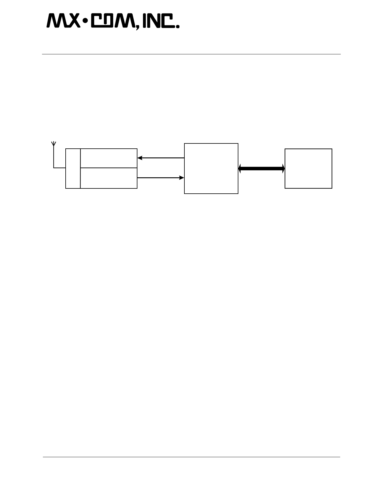
RADIO
MODULATOR
RF
DISCRIMINATOR
ANALOG TX
ANALOG RX
MX909A
MODEM
DATA
PUMP
DATA AND
CONTROL BUS
HOST µC
SYSTEM
APPLICATION
PROCESSING
The MX909A is a low power CMOS device containing all of the baseband signal processing and Medium
Access Control (MAC) protocol functions required for a high performance GMSK Wireless Packet Data
Modem. The MX909A interfaces with a host µC and radio modulation/demodulation circuits to deliver reliable
two-way transfer of application data over a wireless link.
The MX909A assembles application data received from the host µC, adds forward error correction (FEC), and
error detection (CRC) codes, time-spreads this data by interleaving (burst-error protection) and scrambles
(randomizes) the bit pattern. After automatically adding bit and frame sync codewords, the data packet is
converted into analog GMSK signals for modulating into the radio transmitter.
In the receive mode, the MX909A performs the reverse function using the analog signals from the receivers
discriminator. After error correction and removal of the packet overhead, the recovered application data is
supplied to the host µC. Any CRC detected residual uncorrected errors in the data will be flagged. Readout
of the SNR value during receipt of a packet is also provided.
The MX909A uses data block sizes and FEC/CRC algorithms compatible with the Mobitex¥ Wide Area
Network over-air standard. The format used is suitable for other private applications where the high-speed
transfer of data over narrow-band wireless links is required. The MX909A is programmable to operate at
standard bit-rates from a wide choice of XTAL/CLOCK frequencies.
The MX909A may be used with a 3.0V to 5.5V power supply and is available in the following packages:
24-pin SSOP (MX909ADS), 24-pin SOIC (MX909ADW), 24-pin PLCC (MX909ALH), and
24-pin PDIP (MX909AP).
¤2001 MX-COM, Inc.
www.mxcom.com Tel: 800 638 5577 336 744 5050 Fax: 336 744 5054
Doc. # 20480134.005
4800 Bethania Station Road, Winston-Salem, NC 27105-1201 USA All trademarks and service marks are held by their respective companies.
1 page 
GMSK Modem Data Pump
3 External Components
Page 5 of 37
MX909A PRELIMINARY INFORMATION
VDD
IRQ
D7
1
2
24 VDD
C1
23 RXAMPOUT
R2
R1 GMSKIN
D6 3 22 RXIN
D5
D4
D3
4 21 VBIAS
5
6
MX909A 20
19
TXOUT
DOC1
R4 GMSKOUT
D2 7 18 DOC2
D1 8 17 XTAL/CLOCK
D0
9
16 XTAL
C7 C6 C5 C2
RD 10 15 A1
WR
CS
VSS
11
12
A0
14 A0
13 CS
XTAL/CLOCK
17
X1 C3
A1
R3
16
XTAL
C4
Figure 2: Recommended External Components
Component
R1
R2
R3
R4
C1
C2
C3
C4
C5
C6
C7
X1
Notes
1
2
3
3
2
4
4
3
Value
100kΩ
1MΩ
0.1 µF
0.1 µF
Tolerance
±20%
±10%
±20%
±5%
±20%
±20%
±20%
±20%
±10%
±20%
±20%
Recommended External Component Notes:
1. See section 4.1.10.
2. See section 4.1.12.
3. See section 4.4.3.
4. C6 and C7 values should satisfy the following formula:
C (Farads) = 120 x 10-6 / Data Rate (bits/second)
Data Rate (kbits/sec)
C6 / C7 (uF)
4.0 4.8 8.0 9.6 16.0 19.2
0.03 0.022 0.015 0.012 0.0068 0.0068
¤2001 MX-COM, Inc.
www.mxcom.com Tel: 800 638 5577 336 744 5050 Fax: 336 744 5054
Doc. # 20480134.005
4800 Bethania Station Road, Winston-Salem, NC 27105-1201 USA All trademarks and service marks are held by their respective companies.
5 Page 
GMSK Modem Data Pump
Page 11 of 37
MX909A PRELIMINARY INFORMATION
4.4 The Programmer's View
The modem appears to the programmer as 4 write only 8-bit registers shadowed by 3 read only registers,
individual registers being selected by the A0 and A1 chip inputs:
A1 A0
Write to Modem
Read from Modem
00
01
Data Buffer
Command Register
Data Buffer
Status Register
10
11
Control Register
Mode Register
Data Quality Register
not used
4.4.1 Data Buffer
This is an 18-byte read/write buffer which is used to transfer data (as opposed to command, status, mode,
data quality and control information) between the modem and the host µC.
It appears to the µC as a single 8-bit register; the modem ensuring that sequential µC reads or writes to the
buffer are routed to the correct locations within the buffer.
The µC should only access this buffer when the Status Register BFREE (Buffer Free) bit is '1'.
The buffer should only be written to while in Tx mode and read from while in Rx mode (except when loading
Frame Sync detection bytes while in Rx mode).
4.4.2 Command Register
Writing to this register tells the modem to perform a specific action or actions, depending on the setting of the
TASK, AQLEV and AQBC bits.
Command Register
76543210
AQBC AQLEV
Reserved
set to '0 0 0'
TASK
When there is no action to perform and not 'powersaved', the modem will be in an 'idle' state. If the modem is
in transmit mode the input to the Tx filter will be connected to VBIAS. In receive mode the modem will
continue to measure the received data quality and extract bits from the received signal, supplying them to the
de-interleave buffer, otherwise the received data is ignored.
4.4.2.1 Command Register B7: AQBC - Acquire Bit Clock
This bit has no effect in transmit mode.
In receive mode, when a byte with AQBC bit set to '1' is written to the Command Register, and TASK is not
set to RESET, it initiates an automatic sequence designed to achieve bit timing Synchronization with the
received signal as quickly as possible. This involves setting the Phase Locked Loop of the received bit timing
extraction circuits to its widest bandwidth, then gradually reducing the bandwidth as timing Synchronization is
achieved, until the 'normal' value set by the PLLBW bits of the Control Register is reached.
Setting this bit to '0' (or changing it from '1' to '0') has no effect, however note that the acquisition sequence
will be re-started every time that a byte written to the Command Register has the AQBC bit set to '1'.
The AQBC bit will normally be set up to 12 bits before an SFS (Search for Frame Sync) or SFH (Search for
Frame Head) task, however it may also be used independently to re-establish clock Synchronization quickly
after a long fade. Alternatively, an SFS or SFH task may be written to the Command Register with the AQBC
bit '0' if it is known that clock Synchronization does not need to be re-established. More details of the bit clock
acquisition sequence are given in section 5.3.
¤2001 MX-COM, Inc.
www.mxcom.com Tel: 800 638 5577 336 744 5050 Fax: 336 744 5054
Doc. # 20480134.005
4800 Bethania Station Road, Winston-Salem, NC 27105-1201 USA All trademarks and service marks are held by their respective companies.
11 Page | ||
| Páginas | Total 30 Páginas | |
| PDF Descargar | [ Datasheet MX909A.PDF ] | |
Hoja de datos destacado
| Número de pieza | Descripción | Fabricantes |
| MX909A | GMSK Modem Data Pump | CML |
| Número de pieza | Descripción | Fabricantes |
| SLA6805M | High Voltage 3 phase Motor Driver IC. |
Sanken |
| SDC1742 | 12- and 14-Bit Hybrid Synchro / Resolver-to-Digital Converters. |
Analog Devices |
|
DataSheet.es es una pagina web que funciona como un repositorio de manuales o hoja de datos de muchos de los productos más populares, |
| DataSheet.es | 2020 | Privacy Policy | Contacto | Buscar |