|
|
|
PDF NCP3800V Data sheet ( Hoja de datos )
| Número de pieza | NCP3800V | |
| Descripción | SMBus Level 2 Battery Charger | |
| Fabricantes | ON Semiconductor | |
| Logotipo | ||
Hay una vista previa y un enlace de descarga de NCP3800V (archivo pdf) en la parte inferior de esta página. Total 15 Páginas | ||
|
No Preview Available !
NCP3800V
SMBus Level 2 Battery
Charger
The NCP3800V is a highly integrated Lithium−ion battery charger
controller which can be programmed via the SMBus. It can be used to
charge smart batteries and includes three loops for output voltage,
output current and input current. External switch FETs are driven by
internal charge pump drivers.
Features
• High Efficiency Current Sense Circuit
• Level 2 SMBus Controlled
• 2/3/4 Cell Li+ Battery
• 25 Volt Maximum Adapter Input Range
• 5.4 V Charge Pump Driving External N−channel FET Switches
• Internal Loop Compensation
• Highly Accurate Regulation
♦ ±0.5% Charge Voltage Accuracy
♦ ±3.5% Charge Current Accuracy
♦ ±3.5% Adaptor Current Accuracy
• These Devices are Pb−Free, Halogen Free/BFR Free and are RoHS
Compliant
Typical Applications
• Notebook Computers
• Netbook Computers
• Tablet PCs
http://onsemi.com
1
QFN20
MN SUFFIX
CASE 485CP
MARKING DIAGRAM
XXXXX
XXXXX
ALYWG
G
XXXXX = Specific Device Code
A = Assembly Location
L = Wafer Lot
Y = Year
W = Work Week
G = Pb−Free Package
(Note: Microdot may be in either location)
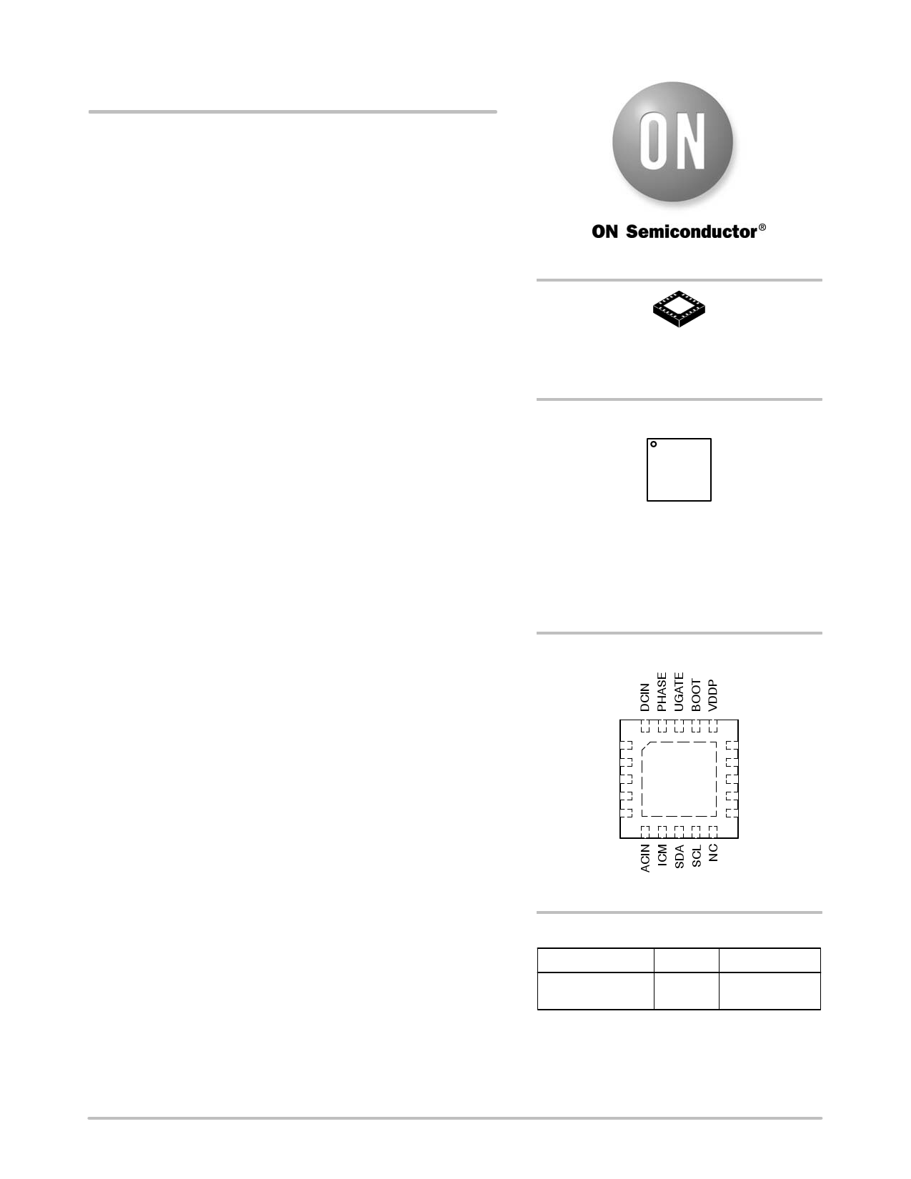
PIN CONFIGURATION
CSSN
CSSP
FETCS
ACFET
ACOK
1
LGATE
GND
CSOP
CSON
BATFET
© Semiconductor Components Industries, LLC, 2013
April, 2013 − Rev. 0
(Top View)
ORDERING INFORMATION
Device
NCP3800VMNTXG
Package
QFN20
(Pb−Free)
Shipping†
3000 / Tape &
Reel
†For information on tape and reel specifications,
including part orientation and tape sizes, please
refer to our Tape and Reel Packaging Specification
Brochure, BRD8011/D.
1 Publication Order Number:
NCP3800V/D
1 page 
NCP3800V
Table 3. ELECTRICAL CHARACTERISTICS
(Unless otherwise noted: DCIN = 20.0 volts, TJ = 0°C to +125°C, Rss = Rso = 10 mW)
Characteristics
Symbol
ICM OUTPUT
ICM output voltage range
ICM output current
ChargeOption()bit9=0, current sense amplifier gain
ChargeOption()bit9=1, current sense amplifier gain
ChargeOption()bit5=0, adaptor current
ChargeOption()bit5=1, charge current
ICM accuracy (Input referred)
ICM accuracy (ChargeCurrent()=0x1000H, 10 mW)
PWM & ERROR AMPLIFIERS
Oscillator Frequency
GATE DRIVE SUPPLY (VDDP)
Output Voltage (Iout = 50 mA)
Output Current (Note 1)
Vddp
Ivddp
Capacitor required for stability (Note 1)
Cvddp
GATE DRIVERS
Lower Gate Drive Source Impedance, 10 mA
R_lgsrc
Lower Gate Drive Sink Impedance, 10 mA
R_lgsnk
Upper Gate Drive Source Impedance, 10 mA
R_ugsrc
Upper Gate Drive Sink Impedance, 10 mA
R_ugsnk
Driver Dead Time, 10 mA
Td
ACFET GATE DRIVER (Charge Pump)
Charge up rising time, 10 nF cap
Gate driver voltage
Vacfet
Gate driver turn−off resistance
BATFET GATE DRIVER (Charge Pump)
Charge up rising time, 10 nF cap
Gate driver voltage
Vacfet
Gate driver turn−off resistance
ACIN COMPARATOR AND ACOK
ACIN Adaptor Detect, Rising Threshold
ACIN Adaptor Detect, Falling Hysteresis
ACIN wakeup threshold rising threshold
ACIN wakeup threshold falling hysteresis
ACOK Rising Delay (deglitch time, default)
ACOK Voltage Drop (Low state, Isink = 1 mA)
ACOK Leakage Current (Open drain, 3.3 V)
(ACOK deglitch time can be programmable by ChargeOption()bit15)
1. Guaranteed by design
Min Typ Max Unit
5.5 V
1 mA
20
40
−1.2
−3
1.2 mV
3%
750 kHz
5.2 5.4 5.6 V
40 mA
0.1 4.7 mF
8 12 W
0.9 1.5 W
6 12 W
0.65 1.3 W
20 ns
1.8
5.0
9
3 ms
V
kW
1.8
5.0
9
3 ms
V
kW
1.96 2.00 2.04
50
0.63
0.05
100 175
250 400
0.5
0: 175 ms(default);1: 1.4s
V
mV
V
V
ms
mV
mA
http://onsemi.com
5
5 Page 
NCP3800V
The data (SDA) and clock (SCL) pins have
Schmitt−trigger inputs that can accommodate slow edges.
Choose pull−up resistors (10 kW) for SDA and SCL to
achieve rise times according to the SMBus specifications.
Communication starts when the master signals a START
condition, which is a high−to−low transition on SDA, while
SCL is high. When the master has finished communicating,
the master issues a STOP condition, which is a low−to−high
transition on SDA, while SCL is high. The bus is then free
for another transmission. The address byte, command byte,
and data bytes are transmitted between the START and
STOP conditions. The SDA state changes only while SCL
is low, except for the START and STOP conditions. Data is
transmitted in 8−bit bytes and is sampled on the rising edge
of SCL. Nine clock cycles are required to transfer each byte
in or out of the NCP3800V because either the master or the
slave acknowledges the receipt of the correct byte during the
ninth clock cycle. The NCP3800V supports the charger
commands as described in the tables of the next section.
Figure 4. SMBus Read and Write Protocols
Figure 5. SMBus Timing Diagrams
http://onsemi.com
11
11 Page | ||
| Páginas | Total 15 Páginas | |
| PDF Descargar | [ Datasheet NCP3800V.PDF ] | |
Hoja de datos destacado
| Número de pieza | Descripción | Fabricantes |
| NCP3800V | SMBus Level 2 Battery Charger | ON Semiconductor |
| Número de pieza | Descripción | Fabricantes |
| SLA6805M | High Voltage 3 phase Motor Driver IC. |
Sanken |
| SDC1742 | 12- and 14-Bit Hybrid Synchro / Resolver-to-Digital Converters. |
Analog Devices |
|
DataSheet.es es una pagina web que funciona como un repositorio de manuales o hoja de datos de muchos de los productos más populares, |
| DataSheet.es | 2020 | Privacy Policy | Contacto | Buscar |