|
|
|
PDF LTC3895 Data sheet ( Hoja de datos )
| Número de pieza | LTC3895 | |
| Descripción | Step-Down DC/DC Controller | |
| Fabricantes | Linear | |
| Logotipo | ||
Hay una vista previa y un enlace de descarga de LTC3895 (archivo pdf) en la parte inferior de esta página. Total 30 Páginas | ||
|
No Preview Available !
LTC3895
150V Low IQ, Synchronous
Step-Down DC/DC Controller
FEATURES
nn Wide VIN Range: 4V to 140V (150V Abs Max)
nn Wide Output Voltage Range: 0.8V to 60V
nn Adjustable Gate Drive Level: 5V to 10V (OPTI-DRIVE)
nn Low Operating IQ: 40μA (Shutdown = 10μA)
nn 100% Duty Cycle Operation
nn No External Bootstrap Diode Required
nn Selectable Gate Drive UVLO Thresholds
nn Onboard LDO or External NMOS LDO for DRVCC
nn EXTVCC LDO Powers Drivers from VOUT
nn Phase-Lockable Frequency (75kHz to 850kHz)
nn Programmable Fixed Frequency (50kHz to 900kHz)
nn Selectable Continuous, Pulse-Skipping or Low Ripple
Burst Mode® Operation at Light Loads
nn Adjustable Burst Clamp and Current Limit
nn Adjustable or Fixed (5V/3.3V) Output Voltage
nn Power Good Output Voltage Monitor
nn Programmable Input Overvoltage Lockout
nn 38-Lead TSSOP High Voltage Package
APPLICATIONS
nn Automotive and Industrial Power Systems
nn High Voltage Battery Operated Systems
nn Telecommunications Power Systems
DESCRIPTION
The LTC®3895 is a high performance step-down switch-
ing regulator DC/DC controller that drives an all N-channel
synchronous power MOSFET stage that can operate from
input voltages up to 140V. A constant frequency current
mode architecture allows a phase-lockable frequency of up
to 850kHz.
The gate drive voltage can be programmed from 5V to 10V
to allow the use of logic or standard-level FETs to maxi-
mize efficiency. An integrated switch in the top gate driver
eliminates the need for an external bootstrap diode. An
internal charge pump allows for 100% duty cycle operation.
The low 40μA no-load quiescent current extends operating
run time in battery-powered systems. OPTI-LOOP® com-
pensation allows the transient response to be optimized
over a wide range of output capacitance and ESR values.
The LTC3895 features a precision 0.8V reference and
power good output indicator. The output voltage can be
programmed between 0.8V to 60V using external resistors
or pin-programmed for a fixed 5V or 3.3V.
L, LT, LTC, LTM, Burst Mode, OPTI-LOOP, PolyPhase, Linear Technology and the Linear
logo are registered trademarks of Linear Technology Corporation. All other trademarks are the
property of their respective owners. Protected by U.S. Patents including 5481178, 5705919,
5929620, 6144194, 6177787, 6580258.
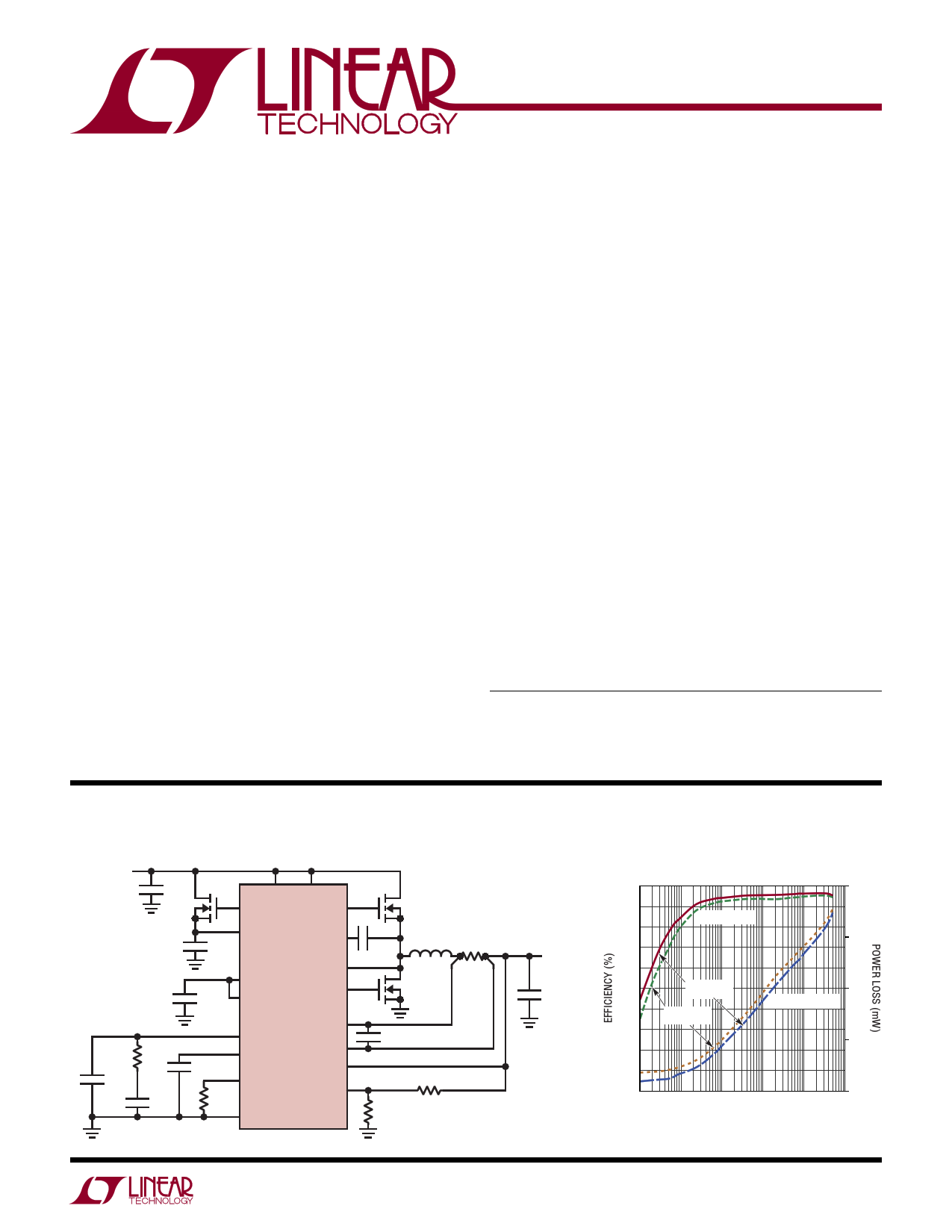
TYPICAL APPLICATION
VIN
7V to 140V
100pF
High Efficiency High Voltage 12V Output Step-Down Regulator
100µF
VIN
NDRV
RUN
TG 0.1µF
DRVCC
4.7µF
BOOST
LTC3895
0.1µF
INTVCC
CPUMP_EN
SW
BG
*VOUT FOLLOWS VIN WHEN VIN < 12V
33µH 6mΩ
VOUT
12V*
5A
150µF
x3
10k
4.7nF
ITH
0.1µF
SS
FREQ
30.1k
GND
SENSE+
SENSE–
EXTVCC
VFB
1nF
511k
36.5k
For more information www.linear.com/LTC3895
Efficiency and Power Loss
vs Load Current
100 10k
90
EFFICIENCY
80
70
1k
60
50 VIN = 24V
40 VIN = 48V
30
20
100
POWER LOSS
10
10
0
0.0001
0.001 0.01 0.1
LOAD CURRENT (A)
1
1 10
3895 TA01b
3895f
1
1 page 
LTC3895
E LECTRICAL CHARACTERISTICS The l denotes the specifications which apply over the specified operating
junction temperature range, otherwise specifications
VPRG = FLOAT unless otherwise noted.
are
at
TA
=
25°C
(Note
2),
VIN
=
12V,
VRUN
=
VIN,
VEXTVCC
=
0V,
VDRVSET
=
0V,
SYMBOL PARAMETER
INTVCC LDO Regulator
VINTVCC
INTVCC Voltage
Oscillator and Phase-Locked Loop
Programmable Frequency
Programmable Frequency
Programmable Frequency
Low Fixed Frequency
High Fixed Frequency
fSYNC
Synchronizable Frequency
PLLIN Input High Level
PLLIN Input Low Level
PGOOD Output
VPGL
IPGOOD
PGOOD Voltage Low
PGOOD Leakage Current
PGOOD Trip Level
Delay for Reporting a Fault
CONDITIONS
ICC = 0mA to 2mA
RFREQ = 25k, PLLIN = DC Voltage
RFREQ = 65k, PLLIN = DC Voltage
RFREQ =105k, PLLIN = DC Voltage
VFREQ = 0V, PLLIN = DC Voltage
VFREQ = INTVCC, PLLIN = DC Voltage
PLLIN = External Clock
PLLIN = External Clock
PLLIN = External Clock
IPGOOD = 2mA
VPGOOD = 3.3V
VFB with Respect to Set Regulated Voltage
VFB Ramping Negative
Hysteresis
VFB with Respect to Set Regulated Voltage
VFB Ramping Positive
Hysteresis
MIN TYP MAX UNITS
4.7 5.0 5.2
V
105
375 440 505
835
320 350 380
485 535 585
l 75
850
l 2.8
l
0.5
kHz
kHz
kHz
kHz
kHz
kHz
V
V
0.02 0.04
10
–13 –10
2.5
–7
7 10 13
2.5
40
V
µA
%
%
%
%
µs
Note 1: Stresses beyond those listed under Absolute Maximum Ratings
may cause permanent damage to the device. Exposure to any Absolute
Maximum Ratings for extended periods may affect device reliability and
lifetime.
Note 2: The LTC3895 is tested under pulsed load conditions such that TJ ≈
TA. The LTC3895E is guaranteed to meet performance specifications from
0°C to 85°C. Specifications over the –40°C to 125°C operating junction
temperature range are assured by design, characterization and correlation
with statistical process controls. The LTC3895I is guaranteed over the
–40°C to 125°C operating junction temperature range and the LTC3895H
is guaranteed over the –40°C to 150°C operating junction temperature
range. Note that the maximum ambient temperature consistent with
these specifications is determined by specific operating conditions in
conjunction with board layout, the rated package thermal impedance
and other environmental factors. High temperatures degrade operating
lifetimes; operating lifetime is derated for junction temperatures greater
than 125ºC. The junction temperature (TJ, in °C) is calculated from the
ambient temperature (TA, in °C) and power dissipation (PD, in Watts)
according to the formula:
TJ = TA + (PD • θJA)
where θJA = 28°C/W for the TSSOP package.
Note 3: This IC includes overtemperature protection that is intended to
protect the device during momentary overload conditions. The maximum
rated junction temperature will be exceeded when this protection is active.
Continuous operation above the specified absolute maximum operating
junction temperature may impair device reliability or permanently damage
the device.
Note 4: The LTC3895 is tested in a feedback loop that servos VITH to a
specified voltage and measures the resultant VFB. The specification at 85°C
is not tested in production and is assured by design, characterization and
correlation to production testing at other temperatures (125°C for the
LTC3895E and LTC3895I, 150°C for the LTC3895H). For the LTC3895I
and LTC3895H, the specification at 0°C is not tested in production and is
assured by design, characterization and correlation to production testing
at –40°C.
Note 5: Dynamic supply current is higher due to the gate charge being
delivered at the switching frequency. See the Applications information
section.
Note 6: Rise and fall times are measured using 10% and 90% levels. Delay
times are measured using 50% levels.
Note 7: The minimum on-time condition is specified for an inductor
peak-to-peak ripple current >40% of IMAX (See Minimum On-Time
Considerations in the Applications Information section).
Note 8: Do not apply a voltage or current source to these pins. They must
be connected to capacitive loads only, otherwise permanent damage may
occur.
Note 9: Do not apply a voltage or current source to the NDRV pin, other
than tying NDRV to DRVCC when not used. If used it must be connected
to capacitive loads only (see DRVCC Regulators in the Applications
Information section), otherwise permanent damage may occur.
Note 10: The minimum input supply operating range is dependent on the
DRVCC UVLO thresholds as determined by the DRVUV pin setting.
3895f
For more information www.linear.com/LTC3895
5
5 Page 
LTC3895
FUNCTIONAL DIAGRAM
PGOOD
OVLO
RUN
MODE
1.2V
15M
3V
CLKOUT
PHASMD
FREQ
20µA
VCO
0.88V
EA–
0.72V
CLK
PFD
EN
CHARGE
PUMP
CPUMP_EN
DRVCC
BOOST
SQ
R
0.425V
DROPOUT
DETECT
BOT
TOPON
SLEEP
TOP
SWITCH
LOGIC
DRVCC
BOT
TG
SW
BG
GND
ICMP
IR
VIN
CB
CIN
L RSENSE
2mV SENSE+
VOUT
COUT
PLLIN
ILIM
100k
DRVSET
20µA
DRVUV
SYNC
DET
CURRENT
LIMIT
2.0V
1.2V
1.8V
BCLAMP
SLOPE COMP
SENSE–
EA– R1
EA 0.80V
SS
R2
VFB
RB
RA
0.88V
VPRG
VPRG
VOUT
R1
FLOAT ADJUSTABLE 0
GND 3.3V FIXED 625k
INTVCC 5V FIXED 1.05M
R2
∞
200k
200k
EXTVCC
VIN
VIN
NDRV
CHARGE
PUMP
EN
DRVCC
NDRV LDO
DRVCC LDO/UVLO
CONTROL
EN
VIN LDO
EN
EXTVCC LDO
4.7V/
7.7V
SHDN
REGSD
ITH
3.5V
10µA
SS
CC1
CC2 RC
CSS
INTVCC
R 4R
INTVCC
LDO
5µA/1uA
For more information www.linear.com/LTC3895
3895f
11
11 Page | ||
| Páginas | Total 30 Páginas | |
| PDF Descargar | [ Datasheet LTC3895.PDF ] | |
Hoja de datos destacado
| Número de pieza | Descripción | Fabricantes |
| LTC3890 | 2-Phase Synchronous Step-Down DC/DC Controller | Linear Technology |
| LTC3890-1 | 2-Phase Synchronous Step-Down DC/DC Controller | Linear |
| LTC3890-2 | 2-Phase Synchronous Step-Down DC/DC Controller | Linear Technology |
| LTC3890-3 | 2-Phase Synchronous Step-Down DC/DC Controller | Linear |
| Número de pieza | Descripción | Fabricantes |
| SLA6805M | High Voltage 3 phase Motor Driver IC. |
Sanken |
| SDC1742 | 12- and 14-Bit Hybrid Synchro / Resolver-to-Digital Converters. |
Analog Devices |
|
DataSheet.es es una pagina web que funciona como un repositorio de manuales o hoja de datos de muchos de los productos más populares, |
| DataSheet.es | 2020 | Privacy Policy | Contacto | Buscar |