|
|
|
PDF XC6190 Data sheet ( Hoja de datos )
| Número de pieza | XC6190 | |
| Descripción | Push Button Reboot Controller | |
| Fabricantes | Torex Semiconductor | |
| Logotipo | ||
Hay una vista previa y un enlace de descarga de XC6190 (archivo pdf) en la parte inferior de esta página. Total 21 Páginas | ||
|
No Preview Available !
XC6190 Series
ETR02031-003
Push Button Reboot Controller
■GENERAL DESCRIPTION
The XC6190 series are timer reset ICs that supply a reboot signal to the system when “L” voltage is input into the
SW1, SW2 pins for a set time (reboot delay time) using two switches (physical buttons).
On type A, the reboot delay time (TDL) can be set as desired by changing the external resistance RT within the range 1s to 20s.
On type B, TDL is fixed internally. When the TS pin is set to “H” level, the delay time is 12.5s. When the TS pin is set to “L”
level, the delay time is 7.5s.
After the reboot signal (TRSTB) is output for 0.4s (TYP), the IC automatically returns to the steady state.
Quiescent current in standby mode is a very small 0.01μA (TYP.), and this contributes to a longer battery drive
time. The small USPN-6 and USPN-6B01 packages enable reduction of mounting space.
The UVLO function is equipped as a protective function to prevent malfunctioning of the IC.
■APPLICATIONS
●Wearable Devices
●Portable Music Players
●Portable Video Game Players
●Wireless Headsets
●Mobile Communication Devices
●Smart Phones, Feature Phones
●Various applications equipped with buttons
■FEATURES
Input Voltage Range
Low power Consumption
Output Configuration
RSTB Pin SINK Current
Reboot Delay Time (Type A)
Reboot Delay Time (Type B)
Reboot Time
Operating Ambient Temperature
Package
Environmentally Friendly
: 1.75V ~ 6.0V
: 0.01μA (Stand-by, TYP.)
: Nch open drain (XC6190AN/BN)
CMOS output (XC6190AC/BC)
: 30mA (VRSTBL=0.3V.)
: 1s ~ 20s (Adjustable by the external resistor)
*12.5s ±5% (RT=200kΩ)
: 7.5s ±5% (TS=GND)
12.5s ±5% (TS=VIN)
: 0.4s±5%
: -40℃ ~ +85℃
: USPN-6, USPN-6B01
: RoHS Compliant, Pb Free
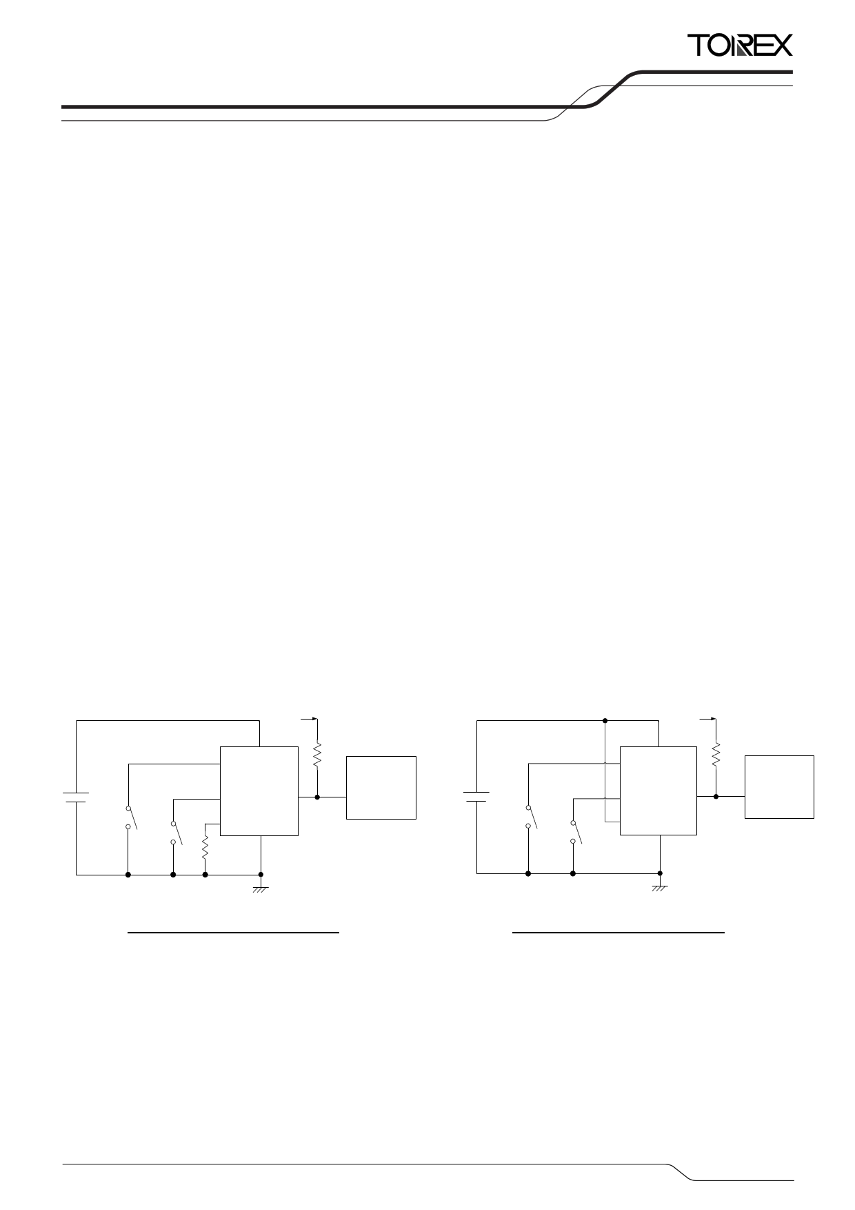
■TYPICAL APPLICATION CIRCUIT
Other
Battery
Button1
Button2
RT
SW1
SW1
VIN
XC6190AN15xx
SW2
RSTB
RT
VSS
RPUL
L
MPU/CPU
RESETB
Battery
Button1
Button2
Other
SW1
SW1
VIN
XC6190BN15xx
SW2
RSTB
TS
VSS
RPUL
L
MPU/CPU
RESETB
A type: Two-Button Solution
B type: Two-Button Solution
*1) On the XC6190AN15xx, XC6190BN25xx, connect a capacitor of at least 0.01μF between VIN-GND near the IC as needed.
*2) On the XC6190AC15xx, XC6190BC25xx, connect a capacitor of at least 0.01μF between VIN-GND near the IC.
(Note) The following products are under development.
XC6190AC158R-G
1/21
1 page 
■PIN CONFIGURATION
XC6190AN15xx / XC6190AC15xx
SW2 6
1 RSTB
RT 5
2 VSS
VIN 4
3 SW1
USPN-6B01
(BOTTOM VIEW)
XC6190BN25xx / XC6190BC25xx
SW2 6
TS 5
VIN 4
1 RSTB
2 VSS
3 SW1
USPN-6B01
(BOTTOM VIEW)
■PIN ASSIGNMENT
PIN NUMBER
USPN-6B01 USPN-6
PIN NAME
11
22
33
44
55
66
RSTB
VSS
SW1
VIN
RT
TS
SW2
XC6190
Series
SW2 6
RT 5
VIN 4
1 RSTB
2 VSS
3 SW1
USPN-6
(BOTTOM VIEW)
SW2 6
TS 5
VIN 4
1 RSTB
2 VSS
3 SW1
USPN-6
(BOTTOM VIEW)
FUNCTIONS
Reboot Signal Output Pin
Ground Pin
Switch Signal(1) Input Pin
Power Input Pin
Type A : TDL adjusting resistor connection Pin
Type B : TDL selection Pin
Switch Signal(2) Input Pin
(Note) The following products are under development.
XC6190AC158R-G
5/21
5 Page 
■ OPERATION EXPLANATION
XC6190
Series
The XC6190 series supplies a reboot signal (TRSTB below) to the system by inputting “L” voltage into the SW1, SW2 pins for
the set time (reboot delay time) using two switches (buttons)
On the XC6190AN15xx and XC6190AC15xx, a reboot delay time (TDL below) is set by connecting a resistance (RT below)
to the RT pin.
TDL is determined by the following calculation formula:
RT(kΩ) = { TDL(s) – 0.097 } / 0.062015 * Can be set within the range 1s to 20s.
e.g.) When TDL=12.5s, RT=200kΩ
On the XC6190BN25xx and XC6190BC25xx, TDL is determined by the internal circuitry. When the TS pin is shorted to VIN,
TDL = 12.5s (TYP.), and when the TS pin is shorted to GND, TDL = 7.5s(TYP.).
Even if the TS pin voltage changes from VIN to GND while “L” voltage is input to the SW1 pin and SW2 pin, the value set
prior to the change is maintained.
VIN
VVUVULVOLRO
0V
VRSTB
0V
Lower than VUVLOR
(Standby mode)
TRSTB
TRSTB
Lower than VUVLO.
(Standby mode)
VSW1
0V
VSW2
0V
TDL
PUSH BUTTON
TDL
PUSH BUTTON
TDL TDL
PUSH BUTTON
TDL
PUSH BUTTON
TDL
PUSH BUTTON
TDL
PUSH BUTTON
TDL
PUSH BUTTON
Details of each circuit part are as follows.
Fig.1_XC6190 Timing Chart
<SW1 pin, SW2 pin>
By inputting “L” voltage into both of these pins during the TDL interval, the reboot signal is output from the RSTB pin.
Both pins are pulled up to VIN by internal resistances, and thus the pin voltage when OPEN is VIN level.
The UVLO circuit is activated by inputting “L” voltage into both the SW1 pin and SW2 pin.
<RT pin: Type A>
RT is connected to this pin to set TDL.
<TS pin: Type B>
This pin is used to set TDL. When the TS pin is shorted to VIN, TDL is set to TDL = 12.5s(TYP.). When the TS pin is shorted
to GND, TDL is set to TDL = 7.5s (TYP.).
Even if the TS pin voltage is changed after “L” voltage is input into both the SW1 and SW2 pins and the internal circuit
starts operation, the value set prior to the change is maintained.
(Note) The following products are under development.
XC6190AC158R-G
11/21
11 Page | ||
| Páginas | Total 21 Páginas | |
| PDF Descargar | [ Datasheet XC6190.PDF ] | |
Hoja de datos destacado
| Número de pieza | Descripción | Fabricantes |
| XC6190 | Push Button Reboot Controller | Torex Semiconductor |
| Número de pieza | Descripción | Fabricantes |
| SLA6805M | High Voltage 3 phase Motor Driver IC. |
Sanken |
| SDC1742 | 12- and 14-Bit Hybrid Synchro / Resolver-to-Digital Converters. |
Analog Devices |
|
DataSheet.es es una pagina web que funciona como un repositorio de manuales o hoja de datos de muchos de los productos más populares, |
| DataSheet.es | 2020 | Privacy Policy | Contacto | Buscar |