|
|
|
PDF ADG5243F Data sheet ( Hoja de datos )
| Número de pieza | ADG5243F | |
| Descripción | Triple SPDT | |
| Fabricantes | Analog Devices | |
| Logotipo | ||
Hay una vista previa y un enlace de descarga de ADG5243F (archivo pdf) en la parte inferior de esta página. Total 30 Páginas | ||
|
No Preview Available !
Data Sheet
User Defined Fault Protection and
Detection, 0.8 pC QINJ, Triple SPDT
ADG5243F
FEATURES
User defined supplies set overvoltage level
Overvoltage protection up to −55 V and +55 V
Power-off protection up to −55 V and +55 V
Overvoltage detection on source pins
Minimum secondary supply level: 4.5 V single-supply
Interrupt flags indicate fault status
Low charge injection (QINJ): 0.8 pC
Low drain/source on capacitance: 10 pF
Latch-up immune under any circumstance
Known state without digital inputs present
VSS to VDD analog signal range
±5 V to ±22 V dual supply operation
8 V to 44 V single-supply operation
Fully specified at ±15 V, ±20 V, +12 V, and +36 V
APPLICATIONS
Analog input/output modules
Process control/distributed control systems
Data acquisition
Instrumentation
Avionics
Automatic test equipment
Communication systems
Relay replacement
GENERAL DESCRIPTION
The ADG5243F comprises three independently selectable, single-
pole/double-throw (SPDT) switches. All channels exhibit break-
before-make switching action that prevents momentary shorting
when switching channels. An EN input enables or disables the
device. When disabled, all channels are switched off. Each switch
conducts equally well in both directions when on, and each
switch has an input signal range that extends to the supplies.
The primary supply voltages define the on-resistance profile,
whereas the secondary supply voltages define the voltage level at
which the overvoltage protection engages.
When no power supplies are present, the channel remains in the
off condition, and the switch inputs are high impedance. Under
normal operating conditions, if the analog input signal levels on
any Sx pin exceed the positive fault voltage (POSFV) or the
negative fault voltage (NEGFV) by a threshold voltage (VT), the
channel turns off and that Sx pin becomes high impedance. If
the switch is selected to be on, then the drain pin is pulled to the
secondary supply voltage that was exceeded. Input signal levels up
to −55 V or +55 V relative to ground are blocked, in both the
powered and unpowered conditions.
Rev. 0
Document Feedback
Information furnished by Analog Devices is believed to be accurate and reliable. However, no
responsibilityisassumedbyAnalogDevices for itsuse,nor foranyinfringementsofpatentsor other
rights of third parties that may result from its use. Specifications subject to change without notice. No
license is granted by implication or otherwise under any patent or patent rights of Analog Devices.
Trademarksandregisteredtrademarksarethepropertyoftheirrespectiveowners.
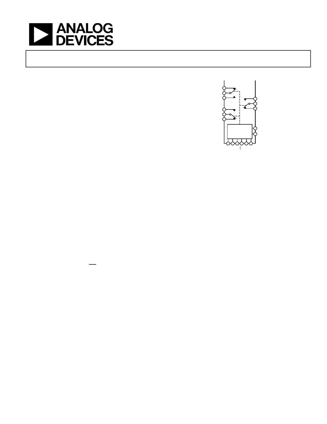
FUNCTIONAL BLOCK DIAGRAM
ADG5243F
S1A
D1
S1B S3B
D3
S2B S3A
D2
S2A
FAULT
DETECTION
AND SWITCH
DRIVER
FF
SF
NOTES
1. SWITCHES SHOWN FOR INPUT LOGIC 1.
Figure 1.
The low capacitance and charge injection of these switches
make them ideal solutions for data acquisition and sample-and-
hold applications, where low glitch switching and fast settling
times are required.
Note that, throughout this data sheet, multifunction pins, such
as IN1/F1, are referred to either by the entire pin name or by a
single function of the pin, for example, IN1, when only that
function is relevant.
PRODUCT HIGHLIGHTS
1. The source pins are protected against voltages greater than
the secondary supply rails, up to −55 V and +55 V.
2. The source pins are protected against voltages between
−55 V and +55 V in an unpowered state.
3. Overvoltage detection with the digital output indicates the
operating state of the switches.
4. Trench isolation guards against latch-up.
5. Optimized for low charge injection and on-capacitance.
6. The ADG5243F can be operated from a dual supply of ±5 V
to ±22 V or a single power supply of 8 V to 44 V.
One Technology Way, P.O. Box 9106, Norwood, MA 02062-9106, U.S.A.
Tel: 781.329.4700
©2015 Analog Devices, Inc. All rights reserved.
Technical Support
www.analog.com
1 page 
Data Sheet
ADG5243F
±20 V DUAL SUPPLY
VDD = 20 V ± 10%, VSS = −20 V ± 10%, GND = 0 V, CDECOUPLING = 0.1 µF, unless otherwise noted.
Table 2.
Parameter
ANALOG SWITCH
Analog Signal Range
On Resistance, RON
On-Resistance Match Between Channels, ∆RON
On-Resistance Flatness, RFLAT(ON)
+25°C
−40°C to
+85°C
−40°C to
+125°C
Unit
270
290 355
250
270 335
1
45
1
45
27
VDD to VSS
410
395
5
5
V
Ω typ
Ω max
Ω typ
Ω max
Ω typ
Ω max
Ω typ
Ω max
Ω typ
29.5 29.5 29.5 Ω max
5 Ω typ
Threshold Voltage, VT
LEAKAGE CURRENTS
Source Off Leakage, IS (Off)
Drain Off Leakage, ID (Off)
Channel On Leakage, ID (On), IS (On)
FAULT
Source Leakage Current, IS
With Overvoltage
6.5 8.5
0.7
±0.1
±1 ±2
±0.1
±1 ±2
±0.3
±1.5 ±5
±66
8.5 Ω max
V typ
nA typ
±5 nA max
nA typ
±5 nA max
nA typ
±10 nA max
µA typ
Power Supplies Grounded or Floating
±25
µA typ
Drain Leakage Current, ID
With Overvoltage
Power Supplies Grounded
Power Supplies Floating
DIGITAL INPUTS/OUTPUTS
Input Voltage
High, VINH
Low, VINL
Input Current, IINL or IINH
Digital Input Capacitance, CIN
Output Voltage
High, VOH
Low, VOL
±2
±8
±5
±100
±50
±15
±100
±50
±50
±100
±50
nA typ
nA max
nA typ
nA max
µA typ
2.0 V min
0.8 V max
±0.7 µA typ
±1.1 ±1.2 µA max
5.0 pF typ
2.0 V min
0.4 V max
Test Conditions/Comments
VDD = +18 V, VSS = −18 V, see Figure 34
VS = ±15 V, IS = −1 mA
VS = ±13.5 V, IS = −1 mA
VS = ±15 V, IS = −1 mA
VS = ±13.5 V, IS = −1 mA
VDD = +20 V, VSS = −20 V, VS = ±15 V, IS =
−1 mA
VDD = +20 V, VSS = −20 V, VS = ±13.5 V, IS =
−1 mA
See Figure 26
VDD = +22 V, VSS = −22 V
VS = ±15 V, VD = ∓15 V, see Figure 32
VS = ±15 V, VD = ∓15 V, see Figure 32
VS = VD = ±15 V, see Figure 33
VDD = +22 V, VSS = −22 V, GND = 0 V,
VS = ±55 V, see Figure 31
VDD = 0 V or floating, VSS = 0 V or floating,
GND = 0 V, INx = 0 V or floating, VS = ±55 V,
see Figure 30
VDD = +22 V, VSS = −22 V, GND = 0 V,
VS = ±55 V, see Figure 31
VDD = 0 V, VSS = 0 V, GND = 0 V, VS = ±55 V,
INx = 0 V, see Figure 30
VDD = floating, VSS = floating, GND = 0 V,
VS = ±55 V, INx = 0 V, see Figure 30
VIN = GND or VDD
Rev. 0 | Page 5 of 30
5 Page 
Data Sheet
CONTINUOUS CURRENT PER CHANNEL, Sx1 OR Dx
Table 5.
Parameter
θJA = 112.6°C/W
25°C
17
10
85°C
11
7
125°C
7
5
1 Sx is the S1A to S3A and S1B to S3B pins.
Unit
mA max
mA max
ADG5243F
Test Conditions/Comments
VS = VSS to VDD − 4.5 V
VS = VSS to VDD
Rev. 0 | Page 11 of 30
11 Page | ||
| Páginas | Total 30 Páginas | |
| PDF Descargar | [ Datasheet ADG5243F.PDF ] | |
Hoja de datos destacado
| Número de pieza | Descripción | Fabricantes |
| ADG5243F | Triple SPDT | Analog Devices |
| Número de pieza | Descripción | Fabricantes |
| SLA6805M | High Voltage 3 phase Motor Driver IC. |
Sanken |
| SDC1742 | 12- and 14-Bit Hybrid Synchro / Resolver-to-Digital Converters. |
Analog Devices |
|
DataSheet.es es una pagina web que funciona como un repositorio de manuales o hoja de datos de muchos de los productos más populares, |
| DataSheet.es | 2020 | Privacy Policy | Contacto | Buscar |