|
|
|
PDF AP6922GMT-HF Data sheet ( Hoja de datos )
| Número de pieza | AP6922GMT-HF | |
| Descripción | DUAL N-CHANNEL ENHANCEMENT MODE POWER MOSFET | |
| Fabricantes | Advanced Power Electronics | |
| Logotipo | ||
Hay una vista previa y un enlace de descarga de AP6922GMT-HF (archivo pdf) en la parte inferior de esta página. Total 8 Páginas | ||
|
No Preview Available !
Advanced Power
Electronics Corp.
AP6922GMT-HF
Halogen-Free Product
DUAL N-CHANNEL MOSFET WITH
SCHOTTKY DIODE
▼ Simple Drive Requirement
▼ Easy for Synchronous Buck
Converter Application
▼ RoHS Compliant & Halogen-Free
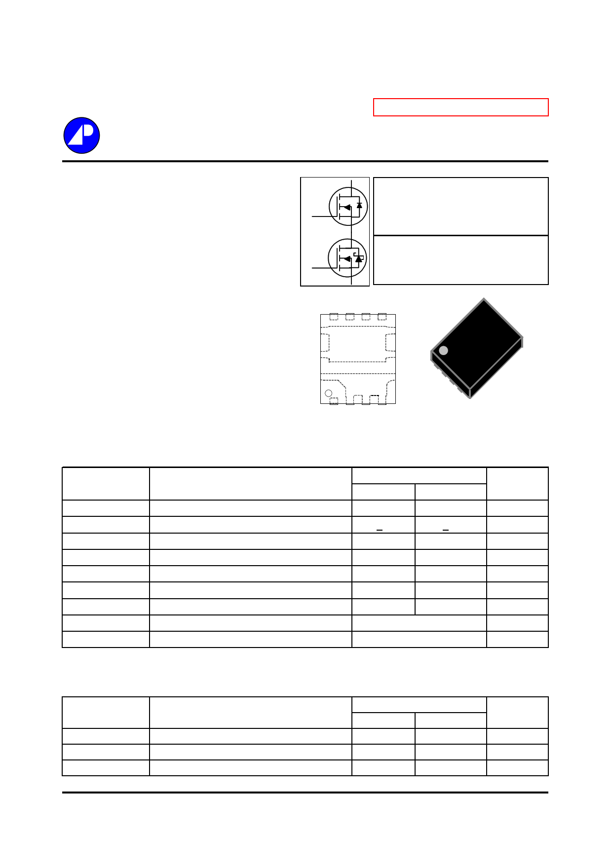
G1
Description
G2
Advanced Power MOSFETs from APEC provide
the designer with the best combination of fast
switching, ruggedized device design, low on-
resistance and cost-effectiveness.
The control MOSFET (CH-1) and synchronous
MOSFET (CH-2) co-package for synchronous buck
converters.
D1 CH-1
D2/S1
CH-2
S2
BVDSS
RDS(ON)
ID
BVDSS
RDS(ON)
ID
G2 S2 S2 S2
S1/D2
30V
8.5mΩ
48A
30V
3.8mΩ
87A
G2
S2
S2
S2
D1
G1 D1 D1 D1
G1
D1
D1
D1
PMPAK® 5x6
Absolute Maximum Ratings@Tj=25oC(unless otherwise specified)
Symbol
Parameter
Rating
Units
CH-1
CH-2
VDS
VGS
ID@TC=25℃
ID@TA=25℃
ID@TA=70℃
IDM
Drain-Source Voltage
Gate-Source Voltage
Drain Current (Chip Limited) , VGS @ 10V
Drain Current3 , VGS @ 10V
Drain Current3 , VGS @ 10V
Pulsed Drain Current1
30
+20
48
15
12
40
30
+12
87
25.7
20.5
60
V
V
A
A
A
A
PD@TA=25℃
TSTG
TJ
Total Power Dissipation
Storage Temperature Range
Operating Junction Temperature Range
3.13 3.9
-55 to 150
-55 to 150
W
℃
℃
Thermal Data
Symbol
Parameter
Rthj-c
Rthj-a
Rthj-a
Maximum Thermal Resistance, Junction-case
Maximum Thermal Resistance, Junction-ambient3
Maximum Thermal Resistance, Junction-ambient4
Data & specifications subject to change without notice
Rating
CH-1
CH-2
4 2.8
40 32
70 60
Units
℃/W
℃/W
℃/W
1
201412173
1 page 
AP6922GMT-HF
Channel-1
10
I D =12A
V DS =15V
8
6
4
2
0
0 2 4 6 8 10 12 14
Q G , Total Gate Charge (nC)
Fig 7. Gate Charge Characteristics
100
Operation in this
area limited by
RDS(ON)
10
100us
1ms
1 10ms
0.1
T A =25 o C
Single Pulse
100ms
1s
DC
0.01
0.01
0.1 1 10
V DS ,Drain-to-Source Voltage (V)
100
Fig 9. Maximum Safe Operating Area
70
V DS =5V
60
50
40
30
20
T j =150 o C
10 T j =25 o C
T j =-40 o C
0
012345
V GS , Gate-to-Source Voltage (V)
Fig 11. Transfer Characteristics
6
f=1.0MHz
1200
1000
800
C600
iss
400
C200
oss
C rss
0
1 5 9 13 17 21 25 29
V DS ,Drain-to-Source Voltage (V)
Fig 8. Typical Capacitance Characteristics
1
Duty factor = 0.5
0.2
0.1 0.1
0.05
0.01
0.02
0.01
Single Pulse
0.001
0.0001
0.001
PDM
t
T
Duty factor = t/T
Peak Tj = PDM x Rthja + Ta
Rthja=70oC/W
0.01 0.1 1 10
t , Pulse Width (s)
100 1000
Fig 10. Effective Transient Thermal Impedance
50
40
30
20
10
0
25 50 75 100 125 150
T C , Case Temperature ( o C )
Fig 12. Drain Current v.s. Case Temperature
5
5 Page | ||
| Páginas | Total 8 Páginas | |
| PDF Descargar | [ Datasheet AP6922GMT-HF.PDF ] | |
Hoja de datos destacado
| Número de pieza | Descripción | Fabricantes |
| AP6922GMT-HF | DUAL N-CHANNEL ENHANCEMENT MODE POWER MOSFET | Advanced Power Electronics |
| Número de pieza | Descripción | Fabricantes |
| SLA6805M | High Voltage 3 phase Motor Driver IC. |
Sanken |
| SDC1742 | 12- and 14-Bit Hybrid Synchro / Resolver-to-Digital Converters. |
Analog Devices |
|
DataSheet.es es una pagina web que funciona como un repositorio de manuales o hoja de datos de muchos de los productos más populares, |
| DataSheet.es | 2020 | Privacy Policy | Contacto | Buscar |