|
|
PDF RT6908 Data sheet ( Hoja de datos )
| Número de pieza | RT6908 | |
| Descripción | PMIC | |
| Fabricantes | Richtek | |
| Logotipo |  |
|
Hay una vista previa y un enlace de descarga de RT6908 (archivo pdf) en la parte inferior de esta página. Total 22 Páginas | ||
|
No Preview Available !
®
RT6908
PMIC for TFT LCD TV Panels
General Description
The RT6908 provides a complete set of programmable
multi-functional power solution for TFT LCD panel. The
RT6908 contains a step-up converter for main power and
step-down controllers to provide the logic voltages for the
system. Moreover, a positive charge pump regulator
provides the adjustable gate-high voltage, VGH; a negative
charge pump regulator provides the gate-low voltage, VGL.
AVDD, VGH and VGL outputs and power sequence can be
programmable through I2C interface.
With its high current capabilities, the device is ideal for
large screen monitor panels and LCD TV applications with
12V supply voltage. The RT6908 is available in a WQFN-
40L 5x5 package.
Ordering Information
RT6908
Package Type
QW : WQFN-40L 5x5 (W-Type)
Lead Plating System
Z : ECO (Ecological Element with
Halogen Free and Pb free)
Note :
Richtek products are :
` RoHS compliant and compatible with the current require-
ments of IPC/JEDEC J-STD-020.
` Suitable for use in SnPb or Pb-free soldering processes.
Marking Information
RT6908ZQW : Product Number
RT6908
ZQW
YMDNN
YMDNN : Date Code
Features
z 9V to 16V Input Supply Voltage
z 4.4A Boost Regulator for AVDD with 12.7V to 19V
Programmable Output
z 1-CH Sync. Buck Converter for VI/O
z 1-CH Sync. Buck Controller for VCORE
z Negative Charge Pump Regulator for VGL with
−8.1V to −1.8V Programmable Output
z Positive Charge Pump Regulator for VGH with 24.5V
to 40V Programmable Output
z Programmable Sequencing
z Voltage Detection Output
z Over Temperature Protection
z I2C Compatible Interface for Register Control
z Thin 40-Lead WQFN Package
z RoHS Compliant and Halogen Free
Applications
z TFT LCD TV Panel
Pin Configurations
(TOP VIEW)
40 39 38 37 36 35 34 33 32 31
PGND 1
30
FBB1 2
29
COMP1 3
28
RSTB 4
27
SDA 5
SCL 6
PGND
26
25
VDET 7
24
AVDD 8
GD 9
41 23
22
LXI 10
21
11 12 13 14 15 16 17 18 19 20
BOOT2
LXB2
DHB2
NC
DLB2
ILIMIT2
FBB2
COMP2
CRST
DRVN
WQFN-40L 5x5
Copyright ©2013 Richtek Technology Corporation. All rights reserved.
DS6908-01 March 2013
is a registered trademark of Richtek Technology Corporation.
www.richtek.com
1
1 page 
Pin No.
28
29
30
31
32
33
34
35
36
38
39
40
RT6908
Pin Name
DHB2
LXB2
BOOT2
EN_I2C
EN
VL
AGND
AVIN
VINB1
BOOT1
LXB1
LXB1
Pin Function
High Side Gate Driver Output for Buck2 Converter.
Buck2 Converter Switch node Between High Side MOSFET and Low Side
MOSFET.
N-MOSFET Gate Drive Voltage for Buck2 Converter. Connect a capacitor
from the switch node LXB2 to this pin.
Enable for I2C Control. AVDD, VGL, VGH enabled by I2C Control.
Chip Enable (Active High). Tie to VL to enable the device.
Internal Logic Regulator Output. Connect this pin with a decoupling
capac itor.
Analog Ground.
Analog Input Voltage of the Device. This is the input for the analog circuits.
Connect this pin with a decoupling capacitor.
Power Input Voltage Pins for the VI/O Buck Converter.
N-MOSFET Gate Drive Voltage for Buck1. Connect a capacitor from the
switch node LXB1 to this pin.
Buck1 Switch node Between High Side MOSFET and Low Side MOSFET.
Buck1 Switch node Between High Side MOSFET and Low Side MOSFET.
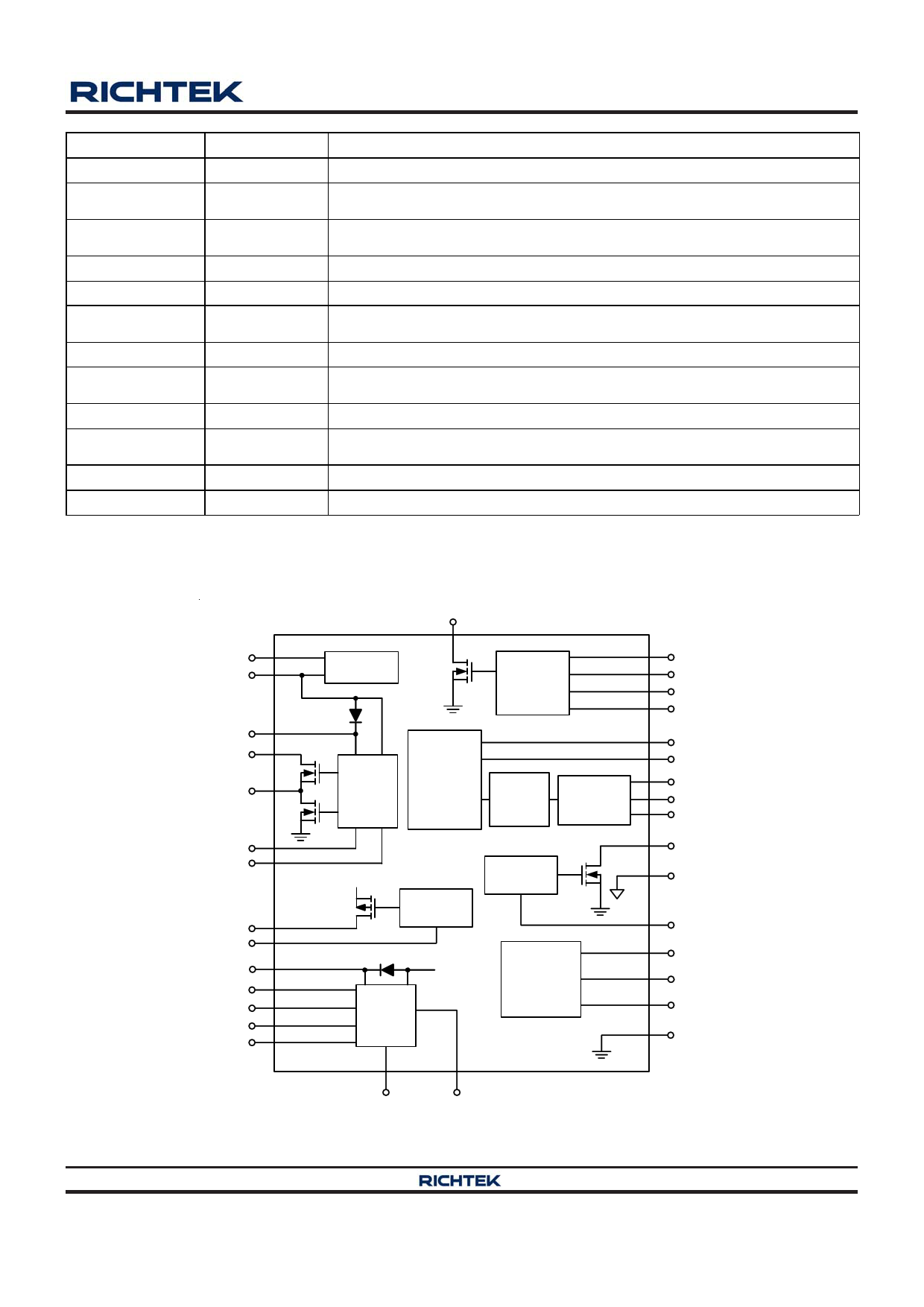
Function Block Diagram
AVIN
VL
Internal
Regulator
LX
BOOST
BOOT1
VINB1
LXB1
FBB1
COMP1
DRVN
VGL
BOOT2
DHB2
LXB2
DLB2
FBB2
Sync.
Buck1
Sequence
Control
DC/DC
DAC
REG
I2C
Interface
VGH
VL Regulator
VGL
Regulator
Sync.
Buck2
VL
Voltage
Detector
LXI
GD
AVDD
COMP
EN
EN_I2C
SDA
SCL
A0
DRVP
AGND
VGH
CRST
RSTB
VDET
PGND
COMP2 ILIMIT2
Copyright ©2013 Richtek Technology Corporation. All rights reserved.
DS6908-01 March 2013
is a registered trademark of Richtek Technology Corporation.
www.richtek.com
5
5 Page 
RT6908
VGH Output Voltage vs. Load Current
38
37
36
35
34
33
0
VIN = 12V, VGH = 35.5V
15 30 45 60
Load Current (mA)
75
Boost Output Voltage vs. Temperature
17.0
16.5
16.0
15.5
15.0
14.5
14.0
-50
-25
VIN = 12V, VAVDD = 15.6V
0 25 50 75 100 125
Temperature (°C)
Buck2 Output Voltage vs. Temperature
1.3
1.2
1.1
1.0
0.9
0.8
-50
-25
VIN = 12V, VCORE = 1.1V
0 25 50 75 100 125
Temperature (°C)
Copyright ©2013 Richtek Technology Corporation. All rights reserved.
DS6908-01 March 2013
VGL Output Voltage vs. Load Current
-3
-4
-5
-6
-7
VIN = 12V, VGL = −6V
-8
0 15 30 45 60 75
Load Current (mA)
Buck1 Output Voltage vs. Temperature
3.5
3.4
3.3
3.2
3.1
3.0
-50
-25
VIN = 12V, VI/O = 3.3V
0 25 50 75
Temperature (°C)
100 125
VGH Output Voltage vs. Temperature
38
37
36
35
34
33
-50
-25
VIN = 12V, VGH = 35.5V
0 25 50 75
Temperature (°C)
100 125
is a registered trademark of Richtek Technology Corporation.
www.richtek.com
11
11 Page | ||
| Páginas | Total 22 Páginas | |
| PDF Descargar | [ Datasheet RT6908.PDF ] | |
Hoja de datos destacado
| Número de pieza | Descripción | Fabricantes |
| RT6908 | PMIC | Richtek |
| Número de pieza | Descripción | Fabricantes |
| SLA6805M | High Voltage 3 phase Motor Driver IC. |
Sanken |
| SDC1742 | 12- and 14-Bit Hybrid Synchro / Resolver-to-Digital Converters. |
Analog Devices |
|
DataSheet.es es una pagina web que funciona como un repositorio de manuales o hoja de datos de muchos de los productos más populares, |
| DataSheet.es | 2020 | Privacy Policy | Contacto | Buscar |
