|
|
|
PDF RT9629B Data sheet ( Hoja de datos )
| Número de pieza | RT9629B | |
| Descripción | Triple-Channel Synchronous Rectified Buck MOSFET Driver | |
| Fabricantes | Richtek | |
| Logotipo | ||
Hay una vista previa y un enlace de descarga de RT9629B (archivo pdf) en la parte inferior de esta página. Total 14 Páginas | ||
|
No Preview Available !
®
RT9629B
Triple-Channel Synchronous Rectified Buck MOSFET
Driver
General Description
The RT9629B is a high frequency, triple-channel
synchronous rectified buck MOSFET driver specifically
designed to drive six power N-MOSFETs. The part is
promoted to pair with Richtek's multiphase buck PWM
controller family for high-density power supply
implementation. The output drivers of RT9629B can
efficiently switch power MOSFETs at frequency 300kHz
typically. Operating in higher frequency should consider
the thermal dissipation carefully. The device implements
bootstrapping on the upper gate with only an external
capacitor and a diode required. This reduces circuit
complexity and allows the use of higher performance, cost
effective N-MOSFETs. All drivers incorporate adaptive
shoot-through protection to prevent upper and lower
MOSFETs from conducting simultaneously and shorting
the input supply. The RT9629B has also detected the fault
condition during initial start-up before the multi-phase PWM
controller takes control. As a result, the input supply will
latch into the shutdown state. The RT9629B comes in a
small footprint package with WQFN-24L 5x5 package.
Features
Drive Six N-MOSFETs for 3-Phase Buck PWM Control
Shoot Through Protection
Embedded Bootstrap Diode
Support High Switching Frequency
Fast Output Rising Time
Tri-State PWM Input for Output Shutdown
Small 24-Lead WQFN Package
RoHS Compliant and Halogen Free
Applications
Core Voltage Supplies for Desktop, Motherboard CPU
High Frequency Low Profile DC/DC Converters
High Current Low Voltage DC/DC Converters
Core Voltage Supplies for GFX Card
Marking Information
RT9629B
ZQW
YMDNN
RT9629BZQW : Product Number
YMDNN : Date Code
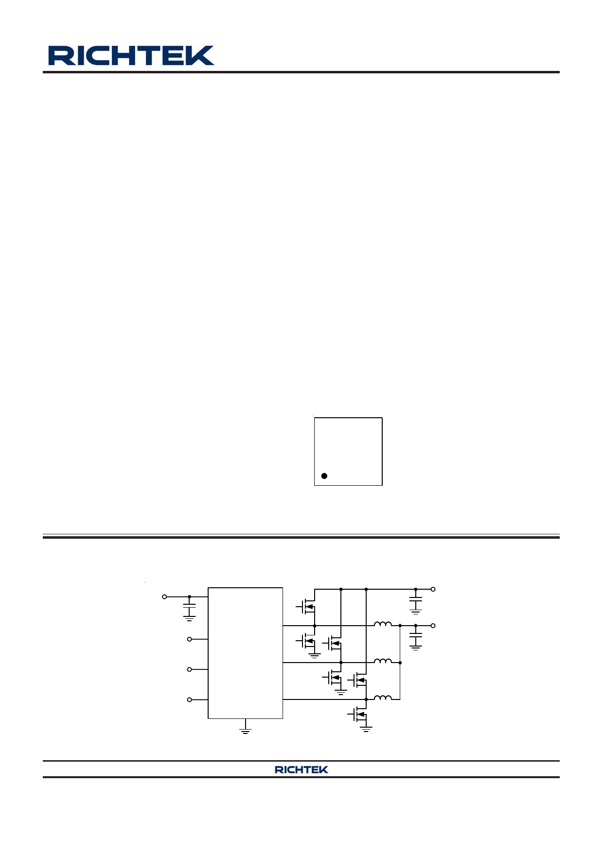
Simplified Application Circuit
12V
PWM1
PWM2
PWM3
VCCx
RT9629B
PHASE1
PWM1
PHASE2
PWM2
PWM3 PHASE3
GND
Copyright ©2014 Richtek Technology Corporation. All rights reserved.
DS9629B-05 April 2014
VIN
L1
VOUT
L2
L3
is a registered trademark of Richtek Technology Corporation.
www.richtek.com
1
1 page 
RT9629B
Absolute Maximum Ratings (Note 1)
Supply Voltage, VCC1, VCC2 --------------------------------------------------------------------- −0.3V to 15V
BOOTx to PHASEx ---------------------------------------------------------------------------------- −0.3V to 15V
PHASEx to GND
DC -------------------------------------------------------------------------------------------------------- −0.3V to 30V
< 20ns --------------------------------------------------------------------------------------------------- −10V to 35V
LGATEx to GND
DC -------------------------------------------------------------------------------------------------------- −0.3V to (VCC + 0.3V)
< 20ns --------------------------------------------------------------------------------------------------- −2V to (VCC + 0.3V)
UGATEx to GND
DC -------------------------------------------------------------------------------------------------------- (VPHASE − 0.3V) to (VBOOT + 0.3V)
< 20ns --------------------------------------------------------------------------------------------------- (VPHASE − 2V) to (VBOOT + 0.3V)
PWMx to GND ---------------------------------------------------------------------------------------- −0.3V to 7V
POR to GND ------------------------------------------------------------------------------------------- −0.3V to 5V
Power Dissipation, PD @ TA = 25°C
WQFN-24L 5x5 --------------------------------------------------------------------------------------- 2.778W
Package Thermal Resistance (Note 2)
WQFN-24L 5x5, θJA ---------------------------------------------------------------------------------- 36°C/W
WQFN-24L 5x5, θJC --------------------------------------------------------------------------------- 6°C/W
Lead Temperature (Soldering, 10 sec.) ---------------------------------------------------------- 260°C
Junction Temperature -------------------------------------------------------------------------------- 150°C
Storage Temperature Range ----------------------------------------------------------------------- −65°C to 150°C
ESD Susceptibility (Note 3)
HBM (Human Body Model) ------------------------------------------------------------------------- 2kV
Recommended Operating Conditions (Note 4)
Supply Voltage, VCC1, VCC2 --------------------------------------------------------------------- 4.5V to 13.2V
Input Voltage, (VIN + VCCx) ----------------------------------------------------------------------- < 35V
Junction Temperature Range ----------------------------------------------------------------------- −40°C to 125°C
Ambient Temperature Range ----------------------------------------------------------------------- −40°C to 85°C
Electrical Characteristics
(VCCx = 12V, TA = 25°C unless otherwise specified)
Parameter
Symbol
Test Conditions
Power Supply Voltage
VCC
Power Supply Current
Power On Reset (POR)
IVCC
VBOOTx = 12V, PWMx Floating
POR Rising Threshold
VPOR_r
VCCx Rising
POR Falling Threshold
VPOR_f
VCCx Falling
POR Pin High Voltage
VPOR_H
POR Pin Low Voltage
VPOR_L
Min Typ Max Unit
4.5 -- 13.2 V
-- 250 -- A
-- 4 4.4 V
3 3.5 --
V
-- 3.5 4
V
-- -- 0.5 V
Copyright ©2014 Richtek Technology Corporation. All rights reserved.
DS9629B-05 April 2014
is a registered trademark of Richtek Technology Corporation.
www.richtek.com
5
5 Page 
RT9629B
d1
VIN
Cgd1
s1
Cgs1
VPHASEx
L
VOUT
Igd1 Igs1
Ig1
g1 g2
Ig2 Igd2
Igs2
Cgd2
d2
D2
Cgs2 s2
Vg1
VPHASEx +12V
GND
Vg2 12V
t
t
Figure 1. Equivalent Circuit and Waveforms (VCC = 12V)
In Figure 1, the current Ig1 and Ig2 are required to move the
gate up to 12V. The operation consists of charging Cgd1,
Cgd2 , Cgs1 and Cgs2. Cgs1 and Cgs2 are the capacitors from
gate to source of the high side and the low side power
MOSFETs, respectively. In general data sheets, the Cgs1
and Cgs2 are referred as “ Ciss” which are the input
capacitors. Cgd1 and Cgd2 are the capacitors from gate to
drain of the high side and the low side power MOSFETs,
respectively and referred to the data sheets as “ Crss” the
reverse transfer capacitance. For example, tr1 and tr2 are
the rising time of the high side and the low side power
MOSFETs respectively, the required current Igs1 and Igs2,
are shown as below :
dVg1 Cgs1 x 12
Igs1 Cgs1 dt
tr1
(1)
dVg2 Cgs1 x 12
Igs2 Cgs1 dt
tr2
(2)
Before driving the gate of the high side MOSFET up to
12V, the low side MOSFET has to be off; and the high
side MOSFET will be turned off before the low side is
turned on. From Figure 1, the body diode “ D2” will be
turned on before high side MOSFETs turn on.
Igd1
= Cgd1
dV
dt
= Cgd1
12
tr1
(3)
Before the low side MOSFET is turned on, the Cgd2 have
been charged to VIN. Thus, as Cgd2 reverses its polarity
and g2 is charged up to 12V, the required current is
Igd2
Cgd2
dV
dt
Cgd2
VIN 12
tr2
(4)
It is helpful to calculate these currents in a typical case.
Assume a synchronous rectified Buck converter, input
voltage VIN = 12V, Vgs1 = 12V, Vgs2 = 12V.The high side
MOSFET is PHB83N03LT whose Ciss = 1660pF,
Crss = 380pF, and tr = 14ns. The low side MOSFET is
PHB95N03LT whose Ciss = 2200pF, Crss = 500pF and
tr = 30ns, from the equation (1) and (2) we can obtain
Igs1
1660 x 10-12 x 12
14 x 10-9
1.428
(A)
(5)
Igs2
2200 x 10-12 x 12 0.88
30 x 10-9
(A)
(6)
from equation. (3) and (4)
Igd1
380 x 10-12 x 12
14 x 10-9
0.326
(A)
500 x 10-12 x 12+12
Igd2
30 x 10-9
0.4 (A)
(7)
(8)
the total current required from the gate driving source can
be calculated as following equations.
Ig1 Igs1 Igd1 1.428 0.326 1.754 (A)
(9)
Ig2 Igs2 Igd2 0.88 0.4 1.28 (A)
(10)
By a similar calculation, we can also get the sink current
required from the turned off MOSFET.
Copyright ©2014 Richtek Technology Corporation. All rights reserved.
DS9629B-05 April 2014
is a registered trademark of Richtek Technology Corporation.
www.richtek.com
11
11 Page | ||
| Páginas | Total 14 Páginas | |
| PDF Descargar | [ Datasheet RT9629B.PDF ] | |
Hoja de datos destacado
| Número de pieza | Descripción | Fabricantes |
| RT9629A | Triple-Channel Synchronous Rectified Buck MOSFET Driver | Richtek |
| RT9629B | Triple-Channel Synchronous Rectified Buck MOSFET Driver | Richtek |
| Número de pieza | Descripción | Fabricantes |
| SLA6805M | High Voltage 3 phase Motor Driver IC. |
Sanken |
| SDC1742 | 12- and 14-Bit Hybrid Synchro / Resolver-to-Digital Converters. |
Analog Devices |
|
DataSheet.es es una pagina web que funciona como un repositorio de manuales o hoja de datos de muchos de los productos más populares, |
| DataSheet.es | 2020 | Privacy Policy | Contacto | Buscar |