|
|
|
PDF RT9722 Data sheet ( Hoja de datos )
| Número de pieza | RT9722 | |
| Descripción | 1.5A Power Switch | |
| Fabricantes | Richtek | |
| Logotipo | ||
Hay una vista previa y un enlace de descarga de RT9722 (archivo pdf) en la parte inferior de esta página. Total 14 Páginas | ||
|
No Preview Available !
RT9722
145mΩ, 1.5A Power Switch with Programmable Current Limit
General Description
The RT9722 is a cost effective, low voltage, single
P-MOSFET high side power switch IC. Typical 145mΩ
switch on resistance and 10μA quiescent current are
realized in this IC. In order to fit different application, a
SET pin is offered for current limit point setting, a resistor
from SET to Ground sets the current limit for this switch.
In addition, the RT9722 integrates a thermal shutdown
circuit and under voltage lockout circuit for overall
protection, and a FLAG output with delay is available to
indicate fault conditions to the local controller.
The RT9722 is an ideal solution for high side power load
switch and can support flexible applications since it is
available in various package such as WDFN-6L 2x2,
SOT-23-5 and SOT-23-6.
Ordering Information
RT9722
Package Type
B : SOT-23-5
E : SOT-23-6
QW : WDFN-6L 2x2 (W-Type)
Lead Plating System
G : Green (Halogen Free and Pb Free)
EN Function
A : Active High
B : Active Low
Note :
Richtek products are :
` RoHS compliant and compatible with the current require-
ments of IPC/JEDEC J-STD-020.
` Suitable for use in SnPb or Pb-free soldering processes.
Features
z Programmable Current Limit : 0.2A to 1.5A
z Low Quiescent Current : 10μA
z Low Shutdown Current : 0.1μA
z 145mΩ Switch On Resistance
z Operating Voltage Range : 2.4V to 5.5V
z Under Voltage Lockout
z Thermal Shutdown Protection
z RoHS Compliant and Halogen Free
Applications
z Handheld Devices
z Hot Swap Supplies
z Notebooks
z Peripheral Ports
z Personal Communication Devices
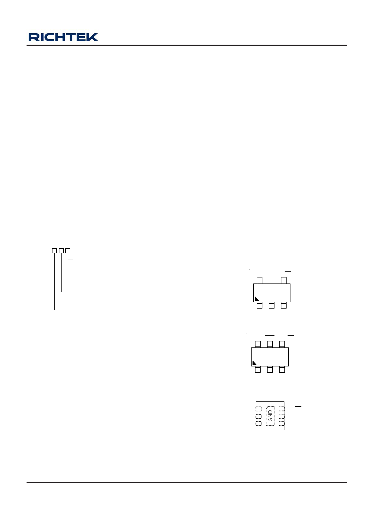
Pin Configurations
(TOP VIEW)
VIN EN/EN
54
23
VOUT GND SET
SOT-23-5
VIN FLG EN/EN
654
23
VOUT GND SET
SOT-23-6
SET 1
VIN 2
VOUT 3
6 EN/EN
5 NC
7 4 FLG
WDFN-6L 2x2
DS9722-00 August 2011
www.richtek.com
1
1 page 
RT9722
Parameter
FLG Output Resistance
FLG Off Current
FLG Delay Time
Under Voltage Lockout
Threshold
Under Voltage Hysteresis
Thermal Shutdown Protection
Thermal Shutdown Hysteresis
Symbol
RFLG
IFLG_Off
tD
VUVLO
ΔVUVLO
TSD
ΔTSD
Test Conditions
ISINK = 1mA
VFLG = 5V
From Fault Condition to FLG
Assertion
VIN Increasing
VIN Increasing
Min Typ Max Unit
-- 20 -- Ω
-- 0.01 1
μA
5 12 20 ms
-- 2 2.4 V
-- 0.1 --
-- 150 --
-- 20 --
V
°C
°C
Note 1. Stresses listed as the above “Absolute Maximum Ratings” may cause permanent damage to the device. These are for
stress ratings. Functional operation of the device at these or any other conditions beyond those indicated in the
operational sections of the specifications is not implied. Exposure to absolute maximum rating conditions for extended
periods may remain possibility to affect device reliability.
Note 2. θJA is measured in the natural convection at TA = 25°C on a low effective thermal conductivity single layer test board of
JEDEC 51-3 thermal measurement standard.
Note 3. Devices are ESD sensitive. Handling precaution is recommended.
Note 4. The device is not guaranteed to function outside its operating conditions.
DS9722-00 August 2011
www.richtek.com
5
5 Page 
RT9722
PD(MAX) = (125°C − 25°C) / (165°C/W) = 0.606W for
WDFN-6L 2x2 package
The maximum power dissipation depends on operating
ambient temperature for fixed TJ(MAX) and thermal
resistance θJA. For the RT9722 Figure 4 shows the
maximum power dissipation allowed under various ambient
temperatures.
0.70 Single Layer PCB
0.60
0.50 WDFN-6L 2x2
0.40
0.30
SOT-23-5/SOT-23-6
0.20
0.10
0.00
0
25 50 75 100
Ambient Temperature (°C)
125
Figure 4. RT9722 Maximum Power Dissipation Derating
Curve
Layout Consideration
For the best performance of the RT9722, careful PCB
layout is necessary. The following guidelines must be
considered:
` Keep all input and output traces as short and wide as
possible.
` Locate the bypass capacitors as close as possible to
the input and output pin of the RT9722.
` Avoid vias as much as possible. If vias are necessary,
make them as large as feasible.
` Place a ground plane under all circuitry to lower both
resistance and inductance and improve DC and transient
performance (Use a separate ground and power plane if
possible).
CIN Rpull-up
The main current
trace should be
as possible as
short and wide.
VIN FLG EN/EN
654
23
VOUT GND SET
The input and output
capacitors should be
placed as close as
COUT RSET
possible to the IC.
Figure 5. PCB Layout Guide
DS9722-00 August 2011
www.richtek.com
11
11 Page | ||
| Páginas | Total 14 Páginas | |
| PDF Descargar | [ Datasheet RT9722.PDF ] | |
Hoja de datos destacado
| Número de pieza | Descripción | Fabricantes |
| RT9721A | 500mA High-Side Power Switches | RichTek |
| RT9721B | 500mA High-Side Power Switches | RichTek |
| RT9722 | 1.5A Power Switch | Richtek |
| RT9724 | 2A Slew Rate Controlled Load Switch | RichTek |
| Número de pieza | Descripción | Fabricantes |
| SLA6805M | High Voltage 3 phase Motor Driver IC. |
Sanken |
| SDC1742 | 12- and 14-Bit Hybrid Synchro / Resolver-to-Digital Converters. |
Analog Devices |
|
DataSheet.es es una pagina web que funciona como un repositorio de manuales o hoja de datos de muchos de los productos más populares, |
| DataSheet.es | 2020 | Privacy Policy | Contacto | Buscar |