|
|
|
PDF RP6102 Data sheet ( Hoja de datos )
| Número de pieza | RP6102 | |
| Descripción | Single Synchronous Buck Controller | |
| Fabricantes | RICHPOWER | |
| Logotipo | ||
Hay una vista previa y un enlace de descarga de RP6102 (archivo pdf) en la parte inferior de esta página. Total 16 Páginas | ||
|
No Preview Available !
RP6102
Single Synchronous Buck Controller
General Description
The RP6102 PWM controller provides high efficiency,
excellent transient response, and high DC output accuracy
needed for stepping down high-voltage batteries to
generate low-voltage CPU core, I/O, and chipset RAM
supplies in notebook computers.
The constant-on-time PWM control scheme handles wide
input/output voltage ratios with ease and provides 100ns
“ instant-on” response to load transients while maintaining
a relatively constant switching frequency.
The RP6102 achieves high efficiency at a reduced cost
by eliminating the current-sense resistor found in
traditional current-mode PWMs. Efficiency is further
enhanced by its ability to drive very large synchronous
rectifier MOSFETs. The buck conversion allows this device
to directly step down high-voltage batteries for the highest
possible efficiency. The RP6102 is intended for CPU core,
chipset, DRAM, or other low-voltage supplies as low as
0.75V.
Features
Ultra-High Efficiency
Resistor Programmable Current Limit by Low-Side
RDS(ON) Sense (Lossless Limit) or Sense Resistor
(High Accuracy)
Quick Load-Step Response within 100ns
1% VOUT Accuracy over Line and Load
Adjustable 0.75V to 3.3V Output Range
4.5V to 26V Battery Input Range
Resistor Programmable Frequency
Over/Under Voltage Protection
2 Steps Current Limit During Soft-Start
Drives Large Synchronous-Rectifier FETs
Power-Good Indicator
RoHS Compliant and 100% Lead (Pb)-Free
Applications
Notebook Computers
CPU Core Supply
Chipset/RAM Supply as Low as 0.75V
Ordering Information
RP6102
Package Type
S : SOP-14
Operating Temperature Range
G : Green (Halogen Free with Commer-
cial Standard)
Note :
Richpower Green products are :
RoHS compliant and compatible with the current
requirements of IPC/JEDEC J-STD-020.
Suitable for use in SnPb or Pb-free soldering processes.
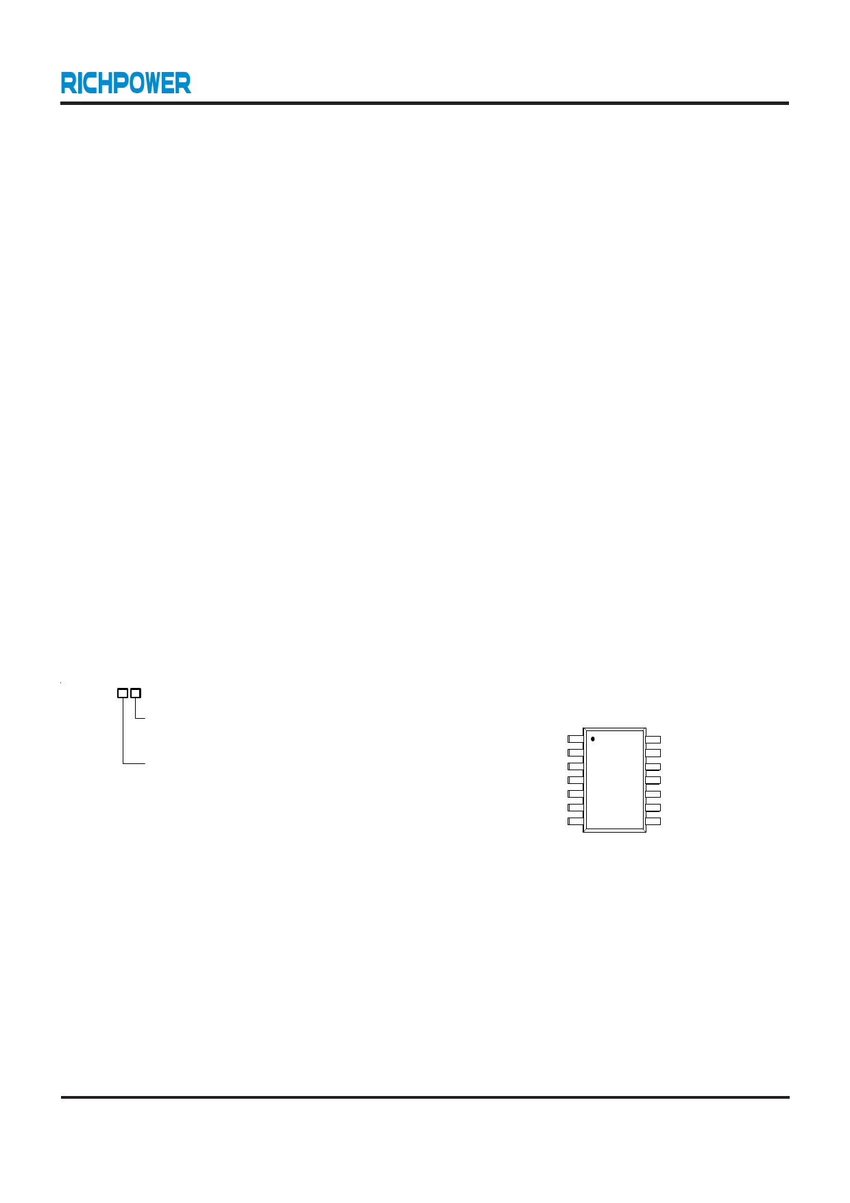
Pin Configurations
(TOP VIEW)
FB
PGOOD
GND
PGND
LGATE
VDDP
OC
14 VDD
2 13 VOUT
3 12 TON
4 11 EN/DEM
5 10 BOOT
6 9 UGATE
7 8 PHASE
SOP-14
Marking Information
For marking information, contact our sales representative
directly or through a Richpower distributor located in your
area, otherwise visit our website for detail.
RP6102-02P July 2009
1
1 page 
RP6102
Pa rame te r
Symbol
Test Conditions
Min Typ Max Units
FB Reference Voltage
FB Input Bias Current
VFB
VDD = 4.5 to 5.5V
FB = 0.75V
0.742 0.75 0.758 V
−1 0.1 1 uA
Output Voltage Range
VOUT
0.75 -- 3.3 V
On-Tim e
Minimum Off-Time
VOUT Shutdown Discharge
Re si sta nce
Current Sensing
ILIM Source Current
VIN = 15V, VOUT = 1.25V, RTON = 1M
267
250
EN/DEM = GND
--
334 401
400 550
20 --
ns
ns
Ω
LGATE = High
18 20 22 uA
Current Comparator Offset
GND − OC
−10 --
10 mV
Current Limit Setting Range RILIM
Zero Crossing Threshold
Fault Protection
GND − PHASE, EN/DEM = 5V
2.5 --
−10 --
10 kΩ
5 mV
Current Limit Sense
V olt age
Output UV Threshold
OVP Threshold
OV Fault Delay
VDD UVLO Threshold
Soft-Start Ramp Time
UV Blank Time
VRILIM
GND − PHASE, RILIM = 2.5k
GND − PHASE, RILIM = 10k
35 50 65 mV
170 200 230 mV
60 70 80 %
With respect to error comparator
threshold
10 15 20 %
FB forced above OV threshold
-- 20 -- us
Rising edge, Hysteresis = 20mV,
PWM disabled below this level
4.1 4.3 4.5 V
From EN high to internal VREF reach
0.71V (0 95%)
--
1.35
--
ms
From EN signal going high
-- 3.1 -- ms
Thermal Shutdown
Thermal Shutdown
Hysteresis
Driver On-R esistance
-- 155 -- °C
-- 10 -- °C
UGATE Driver Pull Up
BOOT − PHASE = 5V
UGATE Driver Sink
LGATE Driver Pull Up
RUGATEsk BOOT − PHASE = 5V
LGATE, High State (Source)
LGATE Driver Pull Down
UGATE Driver Source/Sink
Cu rren t
LGATE Driver Source
Cu rren t
LGATE Driver Sink Current
LGATE, Low State (Sink)
UGAT E − PHASE = 2.5V,
BOOT − PHASE = 5V
LGATE forced to 2.5V
LGATE forced to 2.5V
-- 1.5 5 Ω
-- 1.5 5 Ω
-- 1.5 5 Ω
--
0.6 2.5
Ω
-- 1 -- A
-- 1 -- A
-- 3 -- A
Dead Time
LGATE Rising (PHASE = 1.5V)
UGAT E Rising
-- 30 --
ns
-- 30 --
RP6102-02P July 2009
To be continued
5
5 Page 
RP6102
IL
Slope = (VIN -VOUT) / L
iL, peak
iLoad = iL, peak / 2
IL
IL, peak
ILoad
ILIM
0 tON
t
Figure 1. Boundary condition of CCM/DEM
The switching waveforms may appear noisy and
asynchronous when light loading causes diode-emulation
operation, but this is a normal operating condition that
results in high light-load efficiency. Trade-offs in DEM noise
vs. light-load efficiency are made by varying the inductor
value. Generally, low inductor values produce a broader
efficiency vs. load curve, while higher values result in higher
full-load efficiency (assuming that the coil resistance
remains fixed) and less output voltage ripple. The
disadvantages for using higher inductor values include
larger physical size and degrades load-transient response
(especially at low input-voltage levels).
Forced-CCM Mode (EN/DEM = floating)
The low-noise, forced-CCM mode (EN/DEM = floating)
disables the zero-crossing comparator, which controls the
low-side switch on-time. This causes the low-side gate-
drive waveform to become the complement of the high-
side gate-drive waveform. This in turn causes the inductor
current to reverse at light loads as the PWM loop to
maintain a duty ratio VOUT/VIN. The benefit of forced-CCM
mode is to keep the switching frequency fairly constant,
but it comes at a cost: The no-load battery current can be
up to 10mA to 40mA, depending on the external
MOSFETs.
Current-Limit Setting (OCP)
RP6102 has cycle-by-cycle current limiting control. The
current-limit circuit employs a unique “ valley” current
sensing algorithm. If the magnitude of the current-sense
signal at OC is above the current-limit threshold, the PWM
is not allowed to initiate a new cycle (Figure 2).
RP6102-02P July 2009
0t
Figure 2. Valley Current-Limit
Current sensing of the RP6102 can be accomplished in
two ways. Users can either use a current-sense resistor
or the on-state of the low-side MOSFET (RDS(ON)). For
resistor sensing, a sense resistor is placed between the
source of low-side MOSFET and PGND (Figure 3(a)).
RDS(ON) sensing is more efficient and less expensive
(Figure 3(b)). There is a compromise between current-
limit accuracy and sense resistor power dissipation.
PHASE
LGATE
OC
RILIM
PHASE
LGATE
OC
RILIM
(a) (b)
Figure 3. Current-Sense Methods
In both cases, the RILIM resistor between the OC pin and
PHASE pin sets the over current threshold. This resistor
RILIM is connected to a 20uA current source within the
RP6102 which is turned on when the low-side MOSFET
turns on. When the voltage drop across the sense resistor
or low-side MOSFET equals the voltage across the RILIM
resistor, positive current limit will activate. The high-side
MOSFET will not be turned on until the voltage drop across
the sense element (resistor or MOSFET) falls below the
voltage across the RILIM resistor.
Choose a current limit resistor by following Equation :
RILIM = ILIMIT x RSENSE / 20uA
Carefully observe the PC board layout guidelines to ensure
that noise and DC errors do not corrupt the current-sense
signal seen by OC and PGND. Mount the IC close to the
low-side MOSFET and sense resistor with short, direct
11
11 Page | ||
| Páginas | Total 16 Páginas | |
| PDF Descargar | [ Datasheet RP6102.PDF ] | |
Hoja de datos destacado
| Número de pieza | Descripción | Fabricantes |
| RP6100 | 5V to 12V Single Synchronous Buck PWM Controller | RICHPOWER |
| RP6101 | 5V/12V Synchronous Buck PWM DC-DC Controller | RICHPOWER |
| RP6102 | Single Synchronous Buck Controller | RICHPOWER |
| RP6104 | Wide Input Range Synchronous Buck DC/DC PWM Controller | RichPower |
| Número de pieza | Descripción | Fabricantes |
| SLA6805M | High Voltage 3 phase Motor Driver IC. |
Sanken |
| SDC1742 | 12- and 14-Bit Hybrid Synchro / Resolver-to-Digital Converters. |
Analog Devices |
|
DataSheet.es es una pagina web que funciona como un repositorio de manuales o hoja de datos de muchos de los productos más populares, |
| DataSheet.es | 2020 | Privacy Policy | Contacto | Buscar |