|
|
|
PDF RP54123 Data sheet ( Hoja de datos )
| Número de pieza | RP54123 | |
| Descripción | Earth Leakage Current Detector | |
| Fabricantes | RICHPOWER | |
| Logotipo | ||
Hay una vista previa y un enlace de descarga de RP54123 (archivo pdf) en la parte inferior de esta página. Total 13 Páginas | ||
|
No Preview Available !
Conceptual
RP54123
Earth Leakage Current Detector
General Description
The RP54123 is a semiconductor integrated circuit with
amplifier for a high-speed earth leakage circuit breaker.
The RP54123 circuit for the amplifying parts of earth
leakage circuit breaker consists of differential amplifier,
latch circuit and voltage regulator. It is connected to the
secondary side of the zero-current transformer (ZCT) which
detects leakage current in the both input of the differential
amplifier. Signals amplified by differential amplifier are
integrated by an external capacitor, and connects to the
input terminal of latch circuit with output suitable for the
characteristics of high-speed earth leakage circuit breaker.
Latch circuit keeps low in the output till the input voltage
reaches the fixed level, and output becomes high when
the leakage current more than fixed flows. It drives a
thyristor connected to the output terminal of latch circuit.
Features
Suitable for JIS C 8371
Good temperature characteristics of input
sensitivity current
High input sensitivity (VT = 6.1mV Typ)
Low external component count
High noise and surge-proof
Low power dissipation (Pd = 5mW Typ) and may
be used from 100V to 220V
High mounting density by SIP package with 8 pins
Wide temperature range (TA = -20°C to +80°C)
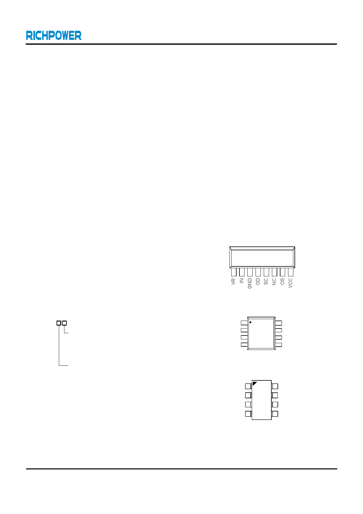
Pin Configurations
(TOP VIEW)
Application
High speed earth leakage circuit breaker
123 45678
Ordering Information
RP54123
Package Type
S : SOP-8
I : SIP-8
V8: SOT-23-8
Operating Temperature Range
G: Green ( Halogen Free with Commer-
cial Standard
Note :
Richpower Green products are :
RoHS compliant and compatible with the current require-
ments of IPC/JEDEC J-STD-020.
Suitable for use in SnPb or Pb-free soldering processes.
SIP-8
VR
IN
GND
NC
2
3
4
8 VCC
7 OS
6 SC
5 OD
SOP-8
NC 8 OD
GND 2 7 SC
IN 3 6 OS
VR 4 5 VCC
SOT-23-8
RP54123-09C Jan 2010
1
1 page 
Conceptual
RP54123
Parameter
Trip Voltage
Timed Current 1
Symbol
VT
ITD1
Test Conditions
VCC = 16V,
VVR - VIN (Note 2)
VCC=16V, VVR-VIN= 30mV
VOD = 1.2V
VCC = 16V, short circuit
Temp-
erature
(°C)
-20 to
80
25
Test
circuit
2
3
Limits (Note 1)
Min Typ Max
Unit
4 6.1 9 mVrms
-12 -- -30 µA
Timed Current 2 ITD2
between VVR and VIN, VOD
= 0.8V
25
4 17 -- 37 µA
Output Current IO
SC “ON” Voltage
(Note 3)
VSC”ON”
VSC=1.6V
VOS=0.8V
ICC1= 580µA
ICC1= 530µA
ICC1= 480µA
VCC = 16V
-20
25
80
25
5 -200 -- --
5 -100 -- -- µA
5
-75 --
--
6 0.7 -- 1.6 V
SC Input Current ISC”ON” VCC = 12V
25 7 -- -- 5 µA
Output Low-level
-20 to
Current
IOSL
VCC = 12V, VOSL = 0.2V
80
8 200 -- -- µA
Input Clamp
-20 to
Voltage
VIC VCC = 12V, IIC = 20mA
9 4.3 -- 6.7 V
80
Differential Input
Clamp Voltage
VID C
IIDC = 100mA
-20 to
80
10
0.4 --
2
V
Max imum
Current Voltage VSM
ISM = 7mA
25 11 20 -- 28 V
Supply Current 2
(Note 4)
ICC2
VVR - VIN VOS = 0.6V
(Note 5)
-20 to
80
12
-- -- 900 µA
Latch Circuit is
Off-state Supply VS”OFF”
Voltage (Note 6)
25 13 0.5 -- -- V
Operating Time
(Note 7)
TON
VCC = 16V,
VVR - VIN = 0.3V
25 14 2 -- 4 ms
Note 1. Typical values are at TA = 25° C.
Note 2. When standard value of voltage (60Hz) between VR and VI is minimum, and output OS is low-level, or when standard
value of voltage (60Hz) between VR and VI is maximum, and output OS is high-level, it is considered as a good one.
Note 3. When standard value of voltage VSC“ ON ” is minimum, and output OS is low-level, or when standard value of voltage
VSC“ ON ” is maximum, and output OS is high-level, it is considered as a good one.
Note 4. Supply current 2 is necessary to keep high in output OS.
Note 5. After applying 30mV between VR and VI and shorting between them, it is considered as a good one if standard value
of IGT flows out of output OS.
Note 6. After supply voltage applies 12V and output OS is high-level, it is considered as a good one in the standard value of
supply voltage and in the low-level of output OS.
Note 7. Operating time is a time from applying fixed input till operating latch circuit in 0.047µF between OD and GND.
RP54123-09C Jan 2010
5
5 Page 
Outline Dimension
Conceptual
RP54123
AC
J
I
B
DFE
H
Symbol
A
B
C
D
E
F
H
I
J
Dimensions In Millimeters
Min
18.90
Max
19.10
6.30
2.70
6.50
2.90
0.35
0.65
0.95
1.45
2.54
0.20
0.35
3.20
11.00
11.40
Dimensions In Inches
Min
0.744
Max
0.752
0.248
0.106
0.256
0.114
0.014
0.026
0.037
0.057
0.100
0.008
0.014
0.126
0.433
0.449
8-Lead SIP Plastic Package
RP54123-09C Jan 2010
11
11 Page | ||
| Páginas | Total 13 Páginas | |
| PDF Descargar | [ Datasheet RP54123.PDF ] | |
Hoja de datos destacado
| Número de pieza | Descripción | Fabricantes |
| RP54123 | Earth Leakage Current Detector | RICHPOWER |
| Número de pieza | Descripción | Fabricantes |
| SLA6805M | High Voltage 3 phase Motor Driver IC. |
Sanken |
| SDC1742 | 12- and 14-Bit Hybrid Synchro / Resolver-to-Digital Converters. |
Analog Devices |
|
DataSheet.es es una pagina web que funciona como un repositorio de manuales o hoja de datos de muchos de los productos más populares, |
| DataSheet.es | 2020 | Privacy Policy | Contacto | Buscar |