|
|
PDF RT5002 Data sheet ( Hoja de datos )
| Número de pieza | RT5002 | |
| Descripción | 7 + 1 Channel DC/DC PMU | |
| Fabricantes | Richtek | |
| Logotipo |  |
|
Hay una vista previa y un enlace de descarga de RT5002 (archivo pdf) en la parte inferior de esta página. Total 30 Páginas | ||
|
No Preview Available !
RT5002
7 + 1 Channel DC/DC PMU with Li-Ion Battery Charger for
DSC
General Description
The RT5002 is a complete power supply solution for digital
still cameras and other handheld devices. It includes a
7+1 channel DC/DC power converter unit, a single-cell Li-
ion battery charger, and an I2C control interface.
The power converter unit includes one synchronous step-
up converter and three synchronous step-down converters
for DSP core, I/O, Motor, and memory power supply, one
synchronous high voltage step-up converter and one
asynchronous inverting converter for CCD± bias, one
WLED driver in either synchronous high voltage step-up
or current source operation, and one low quiescent LDO
for RTC application. All converters are internally frequency
compensated and integrate power MOSFETs. The power
converter unit provides complete protection functions: over
current, thermal shutdown, over voltage, over-load, and
under voltage protection.
The battery charger includes Auto Power Path
Management (APPM). No external MOSFETs are required.
The charger enters sleep mode when power is removed.
Charging tasks are optimized by using a control algorithm
to vary the charge rate, including pre-charge mode, fast
charge mode and constant voltage mode. The charge
current can also be programmed with an external resistor
and modified via the I2C control interface. The scope that
the battery regulation voltage can be modified via the I2C
interface depends on the battery temperature. The internal
thermal feedback circuitry regulates the die temperature
to optimize the charge rate for all ambient temperatures.
The charging task will always be terminated in constant
voltage mode when the charging current reduces to the
termination current of 10% x ICHG_FAST. The charger
includes under voltage and over-voltage protection for the
supply input voltage, VIN.
Applications
DSC
Features
Power Converter Unit :
One Channel LV Sync Step-Up and Three Channel
LV Sync Step-Down
Up to 95% Efficiency
One Sync Step-Up and One Async Inverting for
CCD± bias
One WLED Driver in either Sync Step-Up or Current
Source Operation
WLED Driver with Dimming Control
Step-Up Mode with LED Open Protection (OVP7)
One Low Quiescent LDO with Reverse Leakage
Prevention for RTC Power Supply
Preset On/Off Sequence of CH1, CH2, CH3, CH4
(1 → 3 → 4 → 2)
Two Preset On/Off Sequence of CH5, CH6 (5 → 6 or
6 →5)
All Power Switches Integrated with Internal
Compensation
All Step-Up Converters with Load Disconnect
Wake Up Impulse to Monitor BAT and VIN Plug-In
Charger Unit :
28V Maximum Rating for VIN Power
Selectable Power Current Limit (0.1A / 0.5A / 1.5A)
Auto Power Path Management (APPM) and
Integrated Power MOSFETs
Battery Charging Current Control
Battery Regulation Voltage Control
Programmable Charging Current and Safe Charge
Timer
Under Voltage and Over Voltage Protection
Optimized Charge Rate via Thermal Feedback
Interrupt Indicator to Fault/Status Events
I2C Control Interface : Support Fast Mode up to
400kb/s
Voltage Divider for Sensing Battery Voltage Level
Small 40-Lead WQFN Package
RoHS Compliant and Halogen Free
DS5002-00 November 2011
www.richtek.com
1
1 page 
RT5002
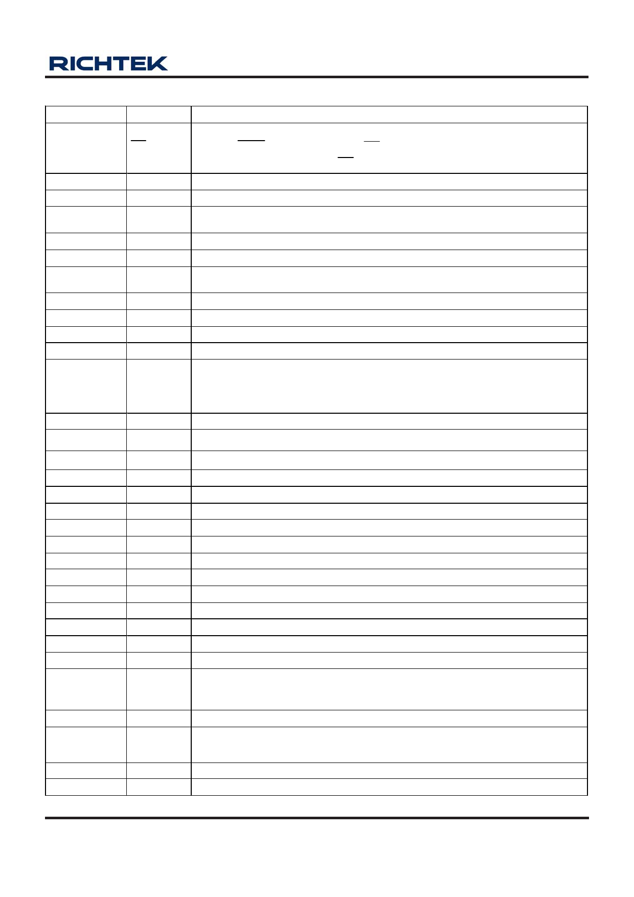
Functional Pin Description
Pin No.
Pin Name
Pin Function
1 INT
Interrupt Indicator Open Drain Output. If any toggle events of TS_FAULT, PGOOD,
EOC, or SAFE happen, the output INT goes low. After I2C register bank address
0x2 is read or power on reset, INT goes high.
2 FB1
Feedback Input of CH1.
3
VDDM
IC Analog Power Pin.
4 FB7
Feedback Input of CH7 in Step-Up Mode or Current Sink Pin of CH7 in Current
Source Mode.
5
PVD7
Power Output of CH7
6 LX7
Switch Node of CH7 in Step-Up Mode.
7
BATS
Output pin of voltage divider for battery voltage level sensing enabled after CH2
soft-start end. BATS voltage is about 60% of BAT.
8 LX4
Switch Node of CH4.
9
PVD4
Power Input of CH4.
10 FB4
Feedback Input of CH4.
11
ISETA
Charge Current Set Input. Connect a resistor (RISETA) between ISETA and GND.
12 TS
Temperature Sense Input. The TS pin connects to a battery’s thermistor to
determine whether the battery is too hot or too cold to be charged. If the battery’s
temperature is out of range, charging is paused until it re-enters the valid range.
TS also detects whether the battery (with NTC) is present or not.
13 VP
Power Output of 3.3V Buffer for Battery Temperature Sensing.
14 SDA
Data Signal Pin of I2C Interface.
15 SCL
Clock Signal Pin of I2C Interface.
16
PVD6
Power Input of CH6.
17 LX6
Switch Node of CH6.
18
VOUT6
Sense Input of CH6 Inverting Output Node.
19 FB6
Feedback Input of CH6.
20
VREF
1.8V Reference Output.
21 FB3
Feedback Input of CH3.
22
PVD3
Power Input of CH3.
23 LX3
Switch Node of CH3.
24 EN1234 Enable Pin of CH1, CH2, CH3, and CH4.
25 FB5
Feedback Input of CH5.
26
PVD5
Power Output of CH5.
27 LX5
Switch Node of CH5.
Input Pin to Select Temperature Sensing Thresholds. Thresholds of TSSEL = H are
28
TSSEL
60% and 38% of VP voltage. Thresholds of TSSEL = L are 74% and 28% of VP
voltage.
29 FB2
Feedback Input of CH2.
30
WAKE
Wake-Up Impulse Push-Pull Output. If VIN or BAT plug in, WAKE pin generates
one 55ms width high pulse to notify micro processor.
31 LX2
Switch Node of CH2.
32
PVD2
Power Input of CH2.
To be continued
DS5002-00 November 2011
www.richtek.com
5
5 Page 
RT5002
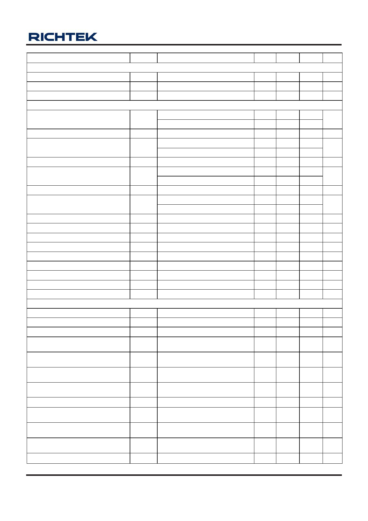
Parameter
Symbol
Test Conditions
Min
Reference
VREF Output Voltage
(VREF-FB6) Regulation Voltage
VREF
1.77
1.182
VREF Load Regulation
0μA < IREF < 200μA
--
Power Switch
CH1 On Resistance of MOSFET
CH1 Current Limitation (Step-Up)
P-MOSFET, VPVD1 = 3.3V
N-MOSFET, VPVD1 = 3.3V
--
--
2.2
CH2 On Resistance of MOSFET
CH2 Current Limitation (Step-Down)
P-MOSFET, VPVD2 = 3.3V
N-MOSFET, VPVD2 = 3.3V
--
--
1.4
CH3 On Resistance of MOSFET
CH3 Current Limitation (Step-Down)
P-MOSFET, VPVD3 = 3.3V
N-MOSFET, VPVD3 = 3.3V
--
--
1.2
CH4 On Resistance of MOSFET
CH4 Current Limitation (Step-Down)
P-MOSFET, VPVD4 = 3.3V
N-MOSFET, VPVD4 = 3.3V
--
--
1.2
CH5 On Resistance of P-MOSFET
CH5 On Resistance of N-MOSFET
CH5 Current Limitation (Step-Up)
VPVD5 = 16V
VDDM = 3.3V
N-MOSFET
--
--
0.9
CH6 On Resistance of MOSFET
CH6 Current Limitation (Inverting)
P-MOSFET, VPVD6 = 3.3V
P-MOSFET
--
1
CH7 On Resistance of P-MOSFET
CH7 On Resistance of N-MOSFET
CH7 Current Limitation (Step-Up)
VPVD7 = 10V
VDDM = 3.3V
N-MOSFET
--
--
0.6
Protection
Over Voltage Protection of PVD1
5.82
Over Voltage Protection of PVD5
20
Over Voltage Protection of VOUT6
Over Voltage Protection of PVD7
(Step-Up mode)
CH1 Step-Up Under Voltage
Protection of PVD1
CH1/2/3/4 Under Voltage Protection
CH5 Under Voltage Protection
CH6 Under Voltage Protection
CH1/2/3/4 Overload Protection
CH5 Overload Protection
CH6 Overload Protection
--
14.2
--
At VFBx < 0.4V after soft-start
ends
At VFB5 < 0.6V after soft-start
ends
At VFB6 > 1.2V after soft-start end
At VFBx < 0.72V after fault delay
(100ms)
At VFB5 < 1.1V after fault delay
(100ms)
At VFB6 > 0.74V after fault delay
(100ms)
0.35
0.5
1.1
0.65
1.05
0.69
Protection Fault Delay
--
Typ
1.8
1.2
--
200
150
3
200
150
1.8
300
300
1.6
300
300
1.6
1.1
0.6
1.2
0.5
1.5
2.0
0.9
0.8
6.0
22
−13
15
VSYS
−0.8V
0.4
0.6
1.2
0.7
1.1
0.74
100
Max
1.83
1.218
10
300
250
4
300
250
2.2
400
400
2
400
400
2
1.5
0.8
1.6
0.7
2
3.0
1.1
1
6.18
24
--
16
--
0.45
0.7
1.3
0.75
1.15
0.79
--
Unit
V
V
mV
mΩ
A
mΩ
A
mΩ
A
mΩ
A
Ω
Ω
A
Ω
A
Ω
Ω
A
V
V
V
V
V
V
V
V
V
V
V
ms
DS5002-00 November 2011
To be continued
www.richtek.com
11
11 Page | ||
| Páginas | Total 30 Páginas | |
| PDF Descargar | [ Datasheet RT5002.PDF ] | |
Hoja de datos destacado
| Número de pieza | Descripción | Fabricantes |
| RT5002 | 7 + 1 Channel DC/DC PMU | Richtek |
| RT5002C | 7 + 1 Channel DC/DC PMU | Richtek |
| RT5006 | Single Output LNB Power Supply Controller | Richtek |
| RT5007 | Single Output LNB Power Supply Controller | Richtek |
| Número de pieza | Descripción | Fabricantes |
| SLA6805M | High Voltage 3 phase Motor Driver IC. |
Sanken |
| SDC1742 | 12- and 14-Bit Hybrid Synchro / Resolver-to-Digital Converters. |
Analog Devices |
|
DataSheet.es es una pagina web que funciona como un repositorio de manuales o hoja de datos de muchos de los productos más populares, |
| DataSheet.es | 2020 | Privacy Policy | Contacto | Buscar |
