|
|
|
PDF RT5007 Data sheet ( Hoja de datos )
| Número de pieza | RT5007 | |
| Descripción | Single Output LNB Power Supply Controller | |
| Fabricantes | Richtek | |
| Logotipo | ||
Hay una vista previa y un enlace de descarga de RT5007 (archivo pdf) en la parte inferior de esta página. Total 20 Páginas | ||
|
No Preview Available !
®
RT5007
Single Output LNB Power Supply Controller with I2C Interface
General Description
The RT5007 is a highly integrated voltage regulator and
interface IC, specifically designed for supplying power and
control signals from advanced satellite Set-Top Box (STB)
modules to the Low Noise Block (LNB) down converter in
the antenna dish or to the multi-switch box.
The device consists of an independent current-mode Boost
controller and low a dropout linear regulator and the circuitry
required for 22kHz tone generation to support one-way
DiSEqCTM communications.
All the functions and the LNB output voltages (8
programmable levels) can be controlled via the I2C bus.
The RT5007 has fault signal to serve as an interrupt for
the processor when any condition turns off the LNB
controller (over current, over temperature and under voltage
lockout). The states of these flags to the faults can be
thoroughly examined through the I2C registers.
Features
Wide Input Supply Voltage Range : 8V to 16V
Wide Output Supply Current Range : 0mA to 500mA
Adjustable Output Current Limit Up to 500mA with
5ms Timer
LNB Voltages (8 Programmable Levels)
±4.5% High Accuracy of LNB Voltage for 0mA to
500mA Current Output
Fault Latch for OTP, OCP, UVLO
Built-in 22kHz Tone Generator One-Way DiSEqCTM
Communication
Adjustable Rising/Falling Time via External
Capacitor
2-Wire Serial I2C Compatible Interface
RoHS Compliant and Halogen Free
Applications
LNB Power Supply and Control for Satellite Set-Top Box
Analog and Digital Satellite Receivers/ Satellite TV,
Satellite PC cards
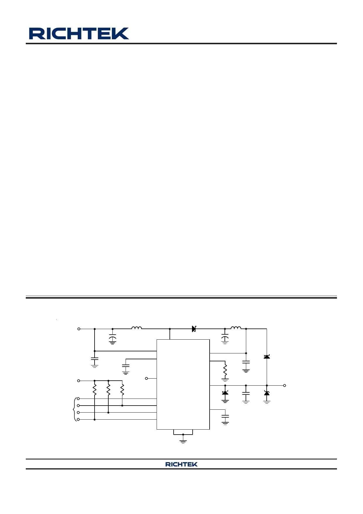
Simplified Application Circuit
VIN
VDD
From
MCU
L1
C1
C2
C3
VA
R1 R2 R3
D1
LX
VIN
VREG
BOOST
ISET
RT5007
ADD
LNB
EXTM
SDA
SCL
IRQ
PGND
TCAP
GND
L2
C4
D3
C5
R4
LNB
Power
D2 C7 D4
C6
Copyright ©2014 Richtek Technology Corporation. All rights reserved.
DS5007-00 July 2014
is a registered trademark of Richtek Technology Corporation.
www.richtek.com
1
1 page 
RT5007
Absolute Maximum Ratings (Note 1)
Supply Input Voltage, VIN ----------------------------------------------------------------------------------------------- −0.3V to 28V
Output Voltage LNB, LX, BOOST ------------------------------------------------------------------------------------- −0.3V to 28V
Other Pins ------------------------------------------------------------------------------------------------------------------ −0.3V to 6V
Power Dissipation, PD @ TA = 25°C
WQFN-16L 3x3 ------------------------------------------------------------------------------------------------------------- 3.33W
Package Thermal Resistance (Note 2)
WQFN-16L 3x3, θJA -------------------------------------------------------------------------------------------------------- 30°C/W
WQFN-16L 3x3, θJC ------------------------------------------------------------------------------------------------------- 7.5°C/W
Junction Temperature ------------------------------------------------------------------------------------------------------ 150°C
Lead Temperature (Soldering, 10 sec.) -------------------------------------------------------------------------------- 260°C
Storage Temperature Range --------------------------------------------------------------------------------------------- −65°C to 150°C
ESD Susceptibility (Note 3)
HBM (Human Body Model) ----------------------------------------------------------------------------------------------- 2kV
MM (Machine Model) ------------------------------------------------------------------------------------------------------ 200V
Recommended Operating Conditions (Note 4)
Supply Input Voltage (Note 5) ---------------------------------------------------------------------------------------- 8V to 16V
Junction Temperature Range -------------------------------------------------------------------------------------------- −40°C to 125°C
Ambient Temperature Range -------------------------------------------------------------------------------------------- −40°C to 85°C
Electrical Characteristics
(VIN = 12V, VLOAD, ILOAD is the output of LNB power, TA = 25°C, unless otherwise specified)
Parameter
Symbol
Test Conditions
Min Typ Max Unit
LNB Output Accuracy,
Load and Line Regulation
Supply Current
Boost Switch On
Resistance
ERR
IIN_OFF
IIN_ON
RDSON
Relative to selected VLNB target level,
ILOAD = 0 to 500mA
ENB bit = 0, LNB output disabled
ENB bit = 1, LNB output enabled,
ILOAD = 0mA
4.5
--
--
--
--
--
4.5 %
10
mA
19
-- 300 600 m
Switching Frequency
fSW
320 352 384 kHz
Switch Current Limit
Linear Regulator Voltage
Drop
VREG output
ILIMSW
VDROP
VREG
VIN = 10V, VBOOST = 19.84V
VBOOST VLNB, no tone signal,
ILOAD = 500mA
-- 3.8 --
A
600 800 1000 mV
-- 5 -- V
TCAP Pin Current
Ripple and Noise on LNB
Output
ICHG
IDISCHG
VRIP_PP
VTCAP = 0V
VTCAP = 4V
20MHz Bandwidth Limit
12.5 10
7.5 10
-- 30
7.5
A
12.5
-- mVPP
Load Regulation
VOUT_LOAD VLNB = 13.667V, ILNB = 50mA to 450mA
VLNB = 19.667V, ILNB = 50mA to 450mA
--
--
38 76
mV
45 90
ISET Voltage
VISET
-- 1 -- V
Copyright ©2014 Richtek Technology Corporation. All rights reserved.
DS5007-00 July 2014
is a registered trademark of Richtek Technology Corporation.
www.richtek.com
5
5 Page 
Application Information
Boost Converter/Linear Regulator
The RT5007 integrates a current mode Boost converter
and linear regulator. Use the I2C to control the LNB voltage
and the Boost converter track is at least greater 800mV
than LNB voltage. The Boost converter is the high
efficiency PWM architecture with 352kHz operation
frequency. The linear regulator has the capability to source
current up to 500mA during continuous operation. All the
loop compensation, current sensing, and slope
compensation functions are provided internally.
The RT5007 has current limiting on the Boost converter
and the LNB output to protect the IC against short circuits.
The internal MOSFET will turn off when the LX current is
higher than 3.8A cycle-by-cycle. If the LNB output in heavy
load, output current is limited to typically 500mA, IRQ
latch to low and the LNB output will be disabled if the over
current condition is more than 5ms. The RT5007 must be
enabled by reading the status register to release the IRQ.
Input Capacitor Selection
The input capacitor reduces voltage spikes from the input
supply and minimizes noise injection to the converter. A
100μF capacitance is sufficient for most applications.
Nevertheless, a higher or lower value may be used
depending on the noise level from the input supply and
the input current to the converter. Note that the voltage
rating of the input capacitor must be greater than the
maximum input voltage.
Inductor Selection
The inductance depends on the maximum input current.
As a general rule, the inductor ripple current range is 20%
to 40% of the maximum input current. If 40% is selected
as an example, the inductor ripple current can be
calculated according to the following equations :
IIN(MAX)
VOUT IOUT(MAX)
VIN
IRIPPLE 0.4 IIN(MAX)
where η is the efficiency of the converter, IIN(MAX) is the
maximum input current, and IRIPPLE is the inductor ripple
RT5007
current. The input peak current can then be obtained by
adding the maximum input current with half of the inductor
ripple current as shown in the following equation :
IPEAK = 1.2 x IIN(MAX)
Note that the saturated current of the inductor must be
greater than IPEAK. The inductance can eventually be
determined according to the following equation :
L VIN 2 VOUT VIN
0.4 VOUT 2 IOUT(MAX) fOSC
where fOSC is the switching frequency. For better system
performance, a shielded inductor is preferred to avoid EMI
problems.
Boost Output Capacitor Selection
The RT5007 Boost regulator is internally compensated
and relies on the inductor and output capacitor value for
overall loop stability. The output capacitor is in the 50μF
to 200μF range with a low ESR, as strongly recommended.
The voltage rating on this capacitor should be in the 25V
to 35V range since it is connected to the Boost VOUT rail.
The output ripple voltage is an important index for
estimating chip performance. This portion consists of two
parts. One is the product of the inductor current with the
ESR of the output capacitor, while the other part is formed
by the charging and discharging process of the output
capacitor. As shown in Figure 1, ΔVOUT1 can be evaluated
based on the ideal energy equalization. According to the
definition of Q, the Q value can be calculated as the
following equation :
Q=
1
2
IIN
1
2
IL
IOUT
IIN
1
2
IL
IOUT
VIN 1
VOUT fOSC
= COUT VOUT1
where fOSC is the switching frequency and ΔIL is the
inductor ripple current. Bring COUT to the left side to
estimate the value of ΔVOUT1 according to the following
equation :
VOUT1
D IOUT
COUT fOSC
Copyright ©2014 Richtek Technology Corporation. All rights reserved.
DS5007-00 July 2014
is a registered trademark of Richtek Technology Corporation.
www.richtek.com
11
11 Page | ||
| Páginas | Total 20 Páginas | |
| PDF Descargar | [ Datasheet RT5007.PDF ] | |
Hoja de datos destacado
| Número de pieza | Descripción | Fabricantes |
| RT5002 | 7 + 1 Channel DC/DC PMU | Richtek |
| RT5002C | 7 + 1 Channel DC/DC PMU | Richtek |
| RT5006 | Single Output LNB Power Supply Controller | Richtek |
| RT5007 | Single Output LNB Power Supply Controller | Richtek |
| Número de pieza | Descripción | Fabricantes |
| SLA6805M | High Voltage 3 phase Motor Driver IC. |
Sanken |
| SDC1742 | 12- and 14-Bit Hybrid Synchro / Resolver-to-Digital Converters. |
Analog Devices |
|
DataSheet.es es una pagina web que funciona como un repositorio de manuales o hoja de datos de muchos de los productos más populares, |
| DataSheet.es | 2020 | Privacy Policy | Contacto | Buscar |