|
|
|
PDF WM8533 Data sheet ( Hoja de datos )
| Número de pieza | WM8533 | |
| Descripción | 24-bit 192kHz Stereo DAC | |
| Fabricantes | Wolfson Microelectronics | |
| Logotipo | ||
Hay una vista previa y un enlace de descarga de WM8533 (archivo pdf) en la parte inferior de esta página. Total 30 Páginas | ||
|
No Preview Available !
w
WM8533
24-bit 192kHz Stereo DAC with 2Vrms Ground Referenced Line Output
DESCRIPTION
The WM8533 is a stereo DAC with integral charge pump and
software control interface. This provides 2Vrms line driver
outputs using a 3.3V power supply rail.
The device features ground-referenced outputs and the use
of a DC servo to eliminate the need for line driving coupling
capacitors and effectively eliminate power on pops and
clicks.
The device is controlled and configured either via the
I2C/SPI compliant serial control interface or a hardware
control interface.
The device supports all common audio sampling rates
between 8kHz and 192kHz using all common MCLK / fs
ratios. Master and slave modes are available and de-
emphasis is also supported.
The WM8533 has a 1.8 to 3.3V tolerant digital interface,
allowing logic up to 3.3V to be connected.
The device is available in a 1.842 x 1.772mm 20-ball WCSP.
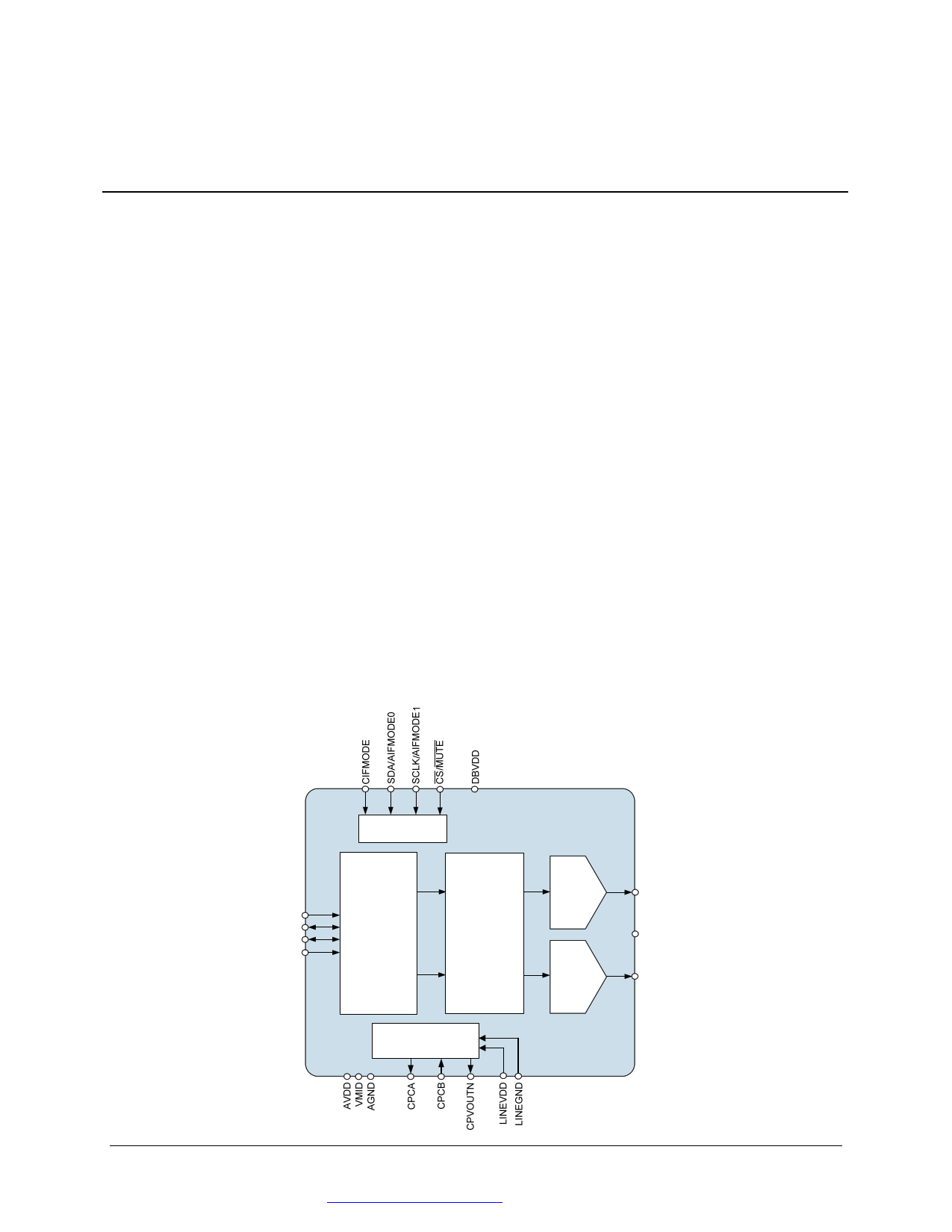
BLOCK DIAGRAM
FEATURES
High performance stereo DAC with ground referenced line
driver
Audio performance
106dB SNR (‘A-weighted’)
-89dB THD @ -1dBFS
Digital volume control ranging from -100dB to +12dB
120dB mute attenuation
All common sample rates from 8kHz to 192kHz supported
I2C/SPI compatible and hardware control modes
Data formats: LJ, RJ, I2S, DSP
De-emphasis supported
Maximum 1mV DC offset on line outputs
Pop/click suppressed power up/down sequencer
AVDD and LINEVDD +3.3V ±10% allowing single supply
DBVDD supply supports +1.8V or +3.3V digital I/O
1.842 x 1.772mm 20-ball WCSP
APPLICATIONS
Consumer digital audio applications requiring 2Vrms output
Set Top Box
Digital TV
DVD Players
Games Consoles
A/V Receivers
MCLK
BCLK
LRCLK
DACDAT
CONTROL
INTERFACE
W
WM8533
DIGITAL
AUDIO
INTERFACE
DIGITAL
FILTERS
LEFT
DAC
RIGHT
DAC
LINEOUTL
LINEREF
LINEOUTR
CHARGE PUMP
WOLFSON MICROELECTRONICS plc
To receive regular email updates, sign up at http://www.wolfsonmicro.com/enews
Production Data, July 2012, Rev 4.0
Copyright 2012 Wolfson Microelectronics plc
1 page 
Production Data
WM8533
ABSOLUTE MAXIMUM RATINGS
Absolute Maximum Ratings are stress ratings only. Permanent damage to the device may be caused by continuously
operating at or beyond these limits. Device functional operating limits and guaranteed performance specifications are given
under Electrical Characteristics at the test conditions specified.
ESD Sensitive Device. This device is manufactured on a CMOS process. It is therefore generically
susceptible to damage from excessive static voltages. Proper ESD precautions must be taken during handling
and storage of this device.
Wolfson tests its package types according to IPC/JEDEC J-STD-020B for Moisture Sensitivity to determine acceptable storage
conditions prior to surface mount assembly. These levels are:
MSL1 = unlimited floor life at <30C / 85% Relative Humidity. Not normally stored in moisture barrier bag.
MSL2 = out of bag storage for 1 year at <30C / 60% Relative Humidity. Supplied in moisture barrier bag.
MSL3 = out of bag storage for 168 hours at <30C / 60% Relative Humidity. Supplied in moisture barrier bag.
The Moisture Sensitivity Level for each package type is specified in Ordering Information.
CONDITION
AVDD, LINEVDD, DBVDD
Voltage range digital inputs
Voltage range analogue inputs
Temperature range, TA
Storage temperature after soldering
MIN
-0.3V
AGND -0.3V
AGND -0.3V
-40°C
-65°C
MAX
+4.5V
DBVDD +0.3V
AVDD +0.3V
+85°C
+150°C
RECOMMENDED OPERATING CONDITIONS
PARAMETER
SYMBOL
TEST CONDITIONS
MIN
TYP
MAX
UNIT
Analogue supply range
AVDD, LINEVDD
2.97 3.3 3.63
V
Digital buffer supply range
DBVDD
1.62 3.63 V
Ground
AGND, LINEGND
0V
Notes
1. Analogue grounds must always be within 0.3V of each other.
2. LINEVDD and AVDD must always be within 0.3V of each other.
w
PD, July 2012, Rev 4.0
5
5 Page 
Production Data
CONTROL INTERFACE TIMING – I2C MODE
I2C mode is selected by driving the CIFMODE pin low.
WM8533
Figure 4 Control Interface Timing – I2C Control Mode
Test Conditions
The following timing information is valid across the full range of recommended operating conditions.
PARAMETER
Program Register Input Information
SCLK Frequency
SCLK Low Pulse-Width
SCLK High Pulse-Width
Hold Time (Start Condition)
Setup Time (Start Condition)
Data Setup Time
SDA, SCLK Rise Time (see Note)
SDA, SCLK Fall Time
Setup Time (Stop Condition)
Data Hold Time
Pulse width of spikes that will be suppressed
Table 3 Control Interface Timing – I2C Control Mode
SYMBOL
t1
t2
t3
t4
t5
t6
t7
t8
t9
MIN TYP
100
100
600
600
100
600
2
Note: When SCLK frequency ≤ 100kHz, the maximum rise time for SDA and SCLK is increased to 1000ns.
MAX
400
300
300
900
8
UNIT
kHz
ns
ns
ns
ns
ns
ns
ns
ns
ns
ns
w
PD, July 2012, Rev 4.0
11
11 Page | ||
| Páginas | Total 30 Páginas | |
| PDF Descargar | [ Datasheet WM8533.PDF ] | |
Hoja de datos destacado
| Número de pieza | Descripción | Fabricantes |
| WM8533 | 24-bit 192kHz Stereo DAC | Wolfson Microelectronics |
| Número de pieza | Descripción | Fabricantes |
| SLA6805M | High Voltage 3 phase Motor Driver IC. |
Sanken |
| SDC1742 | 12- and 14-Bit Hybrid Synchro / Resolver-to-Digital Converters. |
Analog Devices |
|
DataSheet.es es una pagina web que funciona como un repositorio de manuales o hoja de datos de muchos de los productos más populares, |
| DataSheet.es | 2020 | Privacy Policy | Contacto | Buscar |