|
|
|
PDF MUN5311DW1T1 Data sheet ( Hoja de datos )
| Número de pieza | MUN5311DW1T1 | |
| Descripción | Dual Bias Resistor Transistors | |
| Fabricantes | ON Semiconductor | |
| Logotipo | ||
Hay una vista previa y un enlace de descarga de MUN5311DW1T1 (archivo pdf) en la parte inferior de esta página. Total 30 Páginas | ||
|
No Preview Available !
MUN5311DW1T1 Series
Preferred Devices
Dual Bias Resistor
Transistors
NPN and PNP Silicon Surface Mount
Transistors with Monolithic Bias
Resistor Network
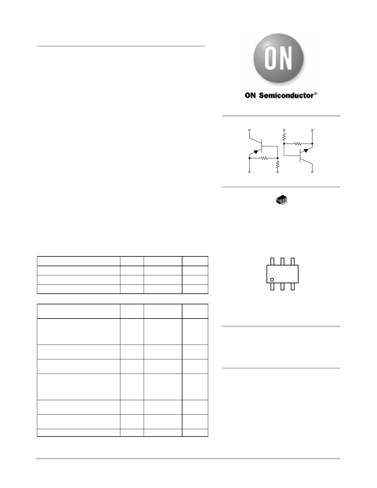
The BRT (Bias Resistor Transistor) contains a single transistor with
a monolithic bias network consisting of two resistors; a series base
resistor and a base−emitter resistor. These digital transistors are
designed to replace a single device and its external resistor bias
network. The BRT eliminates these individual components by
integrating them into a single device. In the MUN5311DW1T1 series,
two complementary BRT devices are housed in the SOT−363 package
which is ideal for low power surface mount applications where board
space is at a premium.
Features
• Simplifies Circuit Design
• Reduces Board Space
• Reduces Component Count
• Available in 8 mm, 7 inch/3000 Unit Tape and Reel
• Pb−Free Package is Available
MAXIMUM RATINGS (TA = 25°C unless otherwise noted, common for Q1
and Q2, − minus sign for Q1 (PNP) omitted)
Rating
Symbol
Value
Unit
Collector-Base Voltage
VCBO
50
Vdc
Collector-Emitter Voltage
VCEO
50
Vdc
Collector Current
IC 100 mAdc
THERMAL CHARACTERISTICS
Characteristic
(One Junction Heated)
Total Device Dissipation
TA = 25°C
Derate above 25°C
Symbol
PD
Thermal Resistance −
Junction-to-Ambient
Characteristic
(Both Junctions Heated)
Total Device Dissipation
TA = 25°C
Derate above 25°C
RqJA
Symbol
PD
Thermal Resistance −
Junction-to-Ambient
Thermal Resistance −
Junction-to-Lead
Junction and Storage Temperature
1. FR−4 @ Minimum Pad
2. FR−4 @ 1.0 x 1.0 inch Pad
RqJA
RqJL
TJ, Tstg
Max
187 (Note 1)
256 (Note 2)
1.5 (Note 1)
2.0 (Note 2)
670 (Note 1)
490 (Note 2)
Max
250 (Note 1)
385 (Note 2)
2.0 (Note 1)
3.0 (Note 2)
493 (Note 1)
325 (Note 2)
188 (Note 1)
208 (Note 2)
−55 to +150
Unit
mW
mW/°C
°C/W
Unit
mW
mW/°C
°C/W
°C/W
°C
© Semiconductor Components Industries, LLC, 2004
September, 2004 − Rev. 9
1
http://onsemi.com
(3) (2) (1)
R1 R2
Q1
R2 R1
Q2
(4) (5)
(6)
6
1
SOT−363
CASE 419B
STYLE 1
MARKING DIAGRAM
6
XXd
1
XX = Specific Device Code
d = Date Code
= (See Page 2)
ORDERING AND DEVICE MARKING
INFORMATION
See detailed ordering, shipping, and specific marking
information in the table on page 2 of this data sheet.
Preferred devices are recommended choices for future use
and best overall value.
Publication Order Number:
MUN5311DW1T1/D
1 page 
MUN5311DW1T1 Series
TYPICAL ELECTRICAL CHARACTERISTICS − MUN5311DW1T1 NPN TRANSISTOR
1
IC/IB = 10
0.1
0.01
TA = −25°C
25°C
75°C
1000
100
VCE = 10 V
TA = 75°C
25°C
−25°C
0.001
0
20 40
IC, COLLECTOR CURRENT (mA)
Figure 2. VCE(sat) versus IC
10
50 1
10
IC, COLLECTOR CURRENT (mA)
Figure 3. DC Current Gain
100
4 100 25°C
f = 1 MHz
75°C
3
IE = 0 V
TA = 25°C
10
TA = −25°C
1
2
0.1
1
0.01
VO = 5 V
0 0 10 20 30 40 50 0.001 0 1 2 3 4 5 6 7 8 9 10
VR, REVERSE BIAS VOLTAGE (VOLTS)
Vin, INPUT VOLTAGE (VOLTS)
Figure 4. Output Capacitance
Figure 5. Output Current versus Input Voltage
10
VO = 0.2 V
1
TA = −25°C
75°C
25°C
0.1
0 10 20 30 40 50
IC, COLLECTOR CURRENT (mA)
Figure 6. Input Voltage versus Output Current
http://onsemi.com
5
5 Page 
MUN5311DW1T1 Series
TYPICAL ELECTRICAL CHARACTERISTICS − MUN5314DW1T1 NPN TRANSISTOR
1
IC/IB = 10
0.1
0.01
TA = −25°C
25°C
75°C
0.001 0
20 40 60
IC, COLLECTOR CURRENT (mA)
Figure 32. VCE(sat) versus IC
80
300
VCE = 10
250
200
150
TA = 75°C
25°C
−25°C
100
50
01 2 4 6 8 10 15 20 40 50 60 70 80 90 100
IC, COLLECTOR CURRENT (mA)
Figure 33. DC Current Gain
4
3.5 f = 1 MHz
lE = 0 V
3 TA = 25°C
2.5
2
1.5
1
0.5
0
0 2 4 6 8 10 15 20 25 30 35 40 45 50
VR, REVERSE BIAS VOLTAGE (VOLTS)
Figure 34. Output Capacitance
100
TA = 75°C
10
25°C
−25°C
VO = 5 V
1
0 2 4 6 8 10
Vin, INPUT VOLTAGE (VOLTS)
Figure 35. Output Current versus Input Voltage
10
VO = 0.2 V
1
TA = −25°C
25°C
75°C
0.1 0 10 20 30 40 50
IC, COLLECTOR CURRENT (mA)
Figure 36. Input Voltage versus Output Current
http://onsemi.com
11
11 Page | ||
| Páginas | Total 30 Páginas | |
| PDF Descargar | [ Datasheet MUN5311DW1T1.PDF ] | |
Hoja de datos destacado
| Número de pieza | Descripción | Fabricantes |
| MUN5311DW1T1 | Dual Bias Resistor Transistors | ON Semiconductor |
| MUN5311DW1T1 | Dual Bias Resistor Transistors | LRC |
| MUN5311DW1T1 | Dual Bias Resistor Transistors | Motorola Semiconductors |
| Número de pieza | Descripción | Fabricantes |
| SLA6805M | High Voltage 3 phase Motor Driver IC. |
Sanken |
| SDC1742 | 12- and 14-Bit Hybrid Synchro / Resolver-to-Digital Converters. |
Analog Devices |
|
DataSheet.es es una pagina web que funciona como un repositorio de manuales o hoja de datos de muchos de los productos más populares, |
| DataSheet.es | 2020 | Privacy Policy | Contacto | Buscar |