|
|
|
PDF MMBZ15VDLT3G Data sheet ( Hoja de datos )
| Número de pieza | MMBZ15VDLT3G | |
| Descripción | 40 Watt Peak Power Zener Transient Voltage Suppressors | |
| Fabricantes | ON Semiconductor | |
| Logotipo | ||
Hay una vista previa y un enlace de descarga de MMBZ15VDLT3G (archivo pdf) en la parte inferior de esta página. Total 5 Páginas | ||
|
No Preview Available !
MMBZxxVxL,
SZMMBZxxVxL Series
40 Watt Peak Power
Zener Transient Voltage
Suppressors
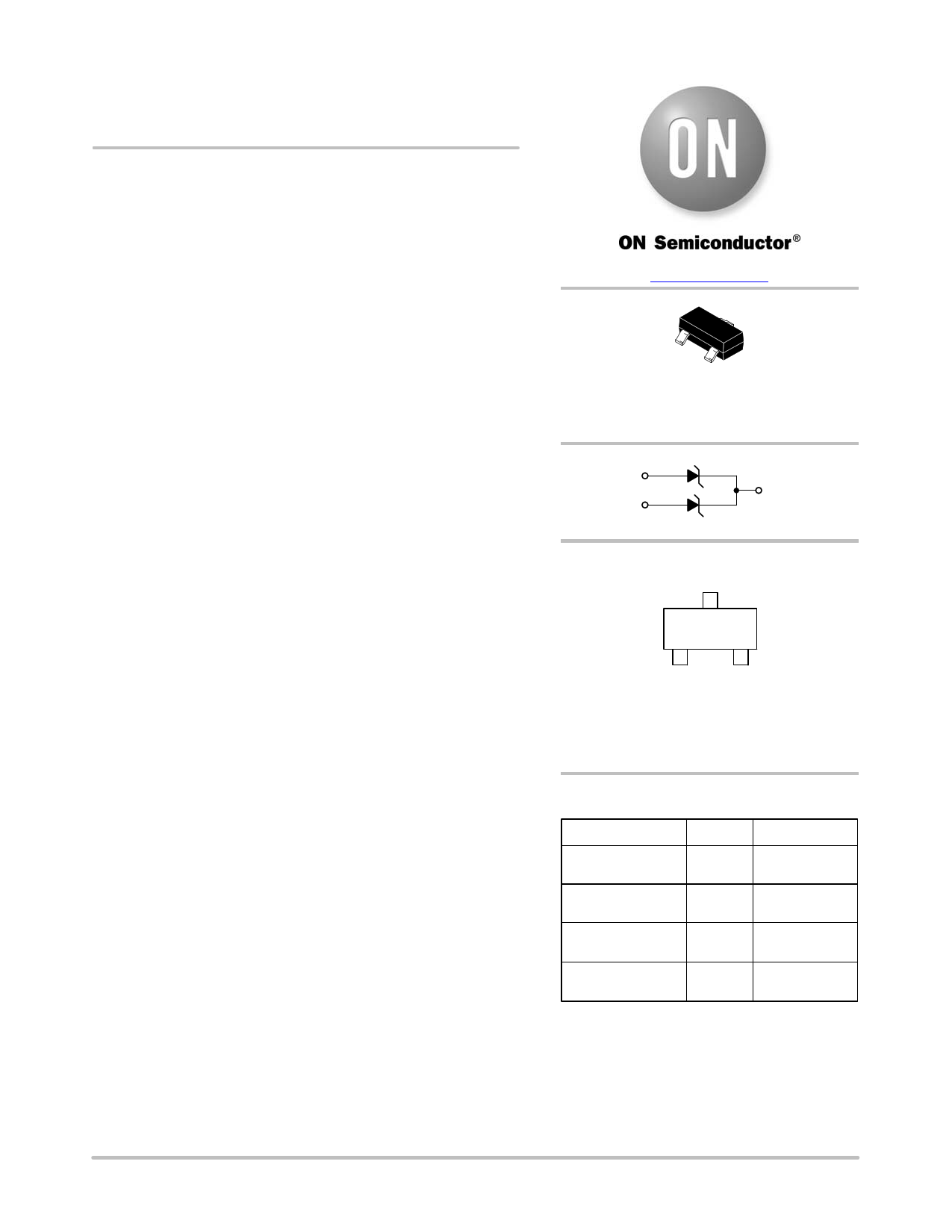
SOT−23 Dual Common Cathode Zeners
for ESD Protection
These dual monolithic silicon zener diodes are designed for
applications requiring transient overvoltage protection capability. They
are intended for use in voltage and ESD sensitive equipment such as
computers, printers, business machines, communication systems,
medical equipment and other applications. Their dual junction common
cathode design protects two separate lines using only one package.
These devices are ideal for situations where board space is at a
premium.
The SZ/MMBZ27VCL can be used to protect a single wire
communication network form EMI and ESD transient surge voltages.
The SZ/MMBZ27VCL is recommended by the
Society of Automotive Engineers (SAE), February 2000, J2411
“Single Wire Can Network for Vehicle Applications” specification as
a solution for transient voltage problems.
Specification Features:
• SOT−23 Package Allows Either Two Separate Unidirectional
Configurations or a Single Bidirectional Configuration
• Working Peak Reverse Voltage Range − 12.8 V, 22 V, 31.2 V
• Standard Zener Breakdown Voltage Range − 15 V, 27 V, 39 V
• Peak Power − 40 W @ 1.0 ms (Bidirectional),
per Figure 5 Waveform
• ESD Rating of Class 3B (exceeding 16 kV) per the Human
Body Model
• ESD Rating of IEC61000−4−2 Level 4, ±30 kV Contact Discharge
• Low Leakage < 100 nA
• Flammability Rating: UL 94 V−O
• SZ Prefix for Automotive and Other Applications Requiring Unique
Site and Control Change Requirements; AEC−Q101 Qualified and
PPAP Capable
• These are Pb−Free Devices
Mechanical Characteristics:
CASE: Void-free, transfer-molded, thermosetting plastic case
FINISH: Corrosion resistant finish, easily solderable
MAXIMUM CASE TEMPERATURE FOR SOLDERING PURPOSES:
260°C for 10 Seconds
www.onsemi.com
SOT−23
CASE 318
STYLE 9
ANODE 1
ANODE 2
3 CATHODE
MARKING DIAGRAM
XXX MG
G
1
XXX = 15D, 27C or 39C
M = Date Code
G = Pb−Free Package
(Note: Microdot may be in either location)
ORDERING INFORMATION
Device
Package
MMBZ15VDLT1G, SOT−23
SZMMBZ15VDLT1G (Pb−Free)
MMBZ15VDLT3G, SOT−23
SZMMBZ15VDLT3G (Pb−Free)
MMBZxxVCLT1G, SOT−23
SZMMBZxxVCLT1G (Pb−Free)
MMBZxxVCLT3G, SOT−23
SZMMBZxxVCLT3G (Pb−Free)
Shipping†
3,000 /
Tape & Reel
10,000 /
Tape & Reel
3,000 /
Tape & Reel
10,000 /
Tape & Reel
†For information on tape and reel specifications,
including part orientation and tape sizes, please
refer to our Tape and Reel Packaging Specifications
Brochure, BRD8011/D.
© Semiconductor Components Industries, LLC, 2015
September, 2015 − Rev. 15
1
Publication Order Number:
MMBZ15VDLT1/D
1 page 
MMBZxxVxL, SZMMBZxxVxL Series
PACKAGE DIMENSIONS
E
A
A1
D
3
12
e
HE
b
SEE VIEW C
SOT−23 (TO−236)
CASE 318−08
ISSUE AP
c
0.25
q
L
L1
VIEW C
NOTES:
1. DIMENSIONING AND TOLERANCING PER ANSI Y14.5M, 1982.
2. CONTROLLING DIMENSION: INCH.
3. MAXIMUM LEAD THICKNESS INCLUDES LEAD FINISH
THICKNESS. MINIMUM LEAD THICKNESS IS THE MINIMUM
THICKNESS OF BASE MATERIAL.
4. DIMENSIONS D AND E DO NOT INCLUDE MOLD FLASH,
PROTRUSIONS, OR GATE BURRS.
MILLIMETERS
DIM MIN NOM MAX
A 0.89
1.00
1.11
A1 0.01
0.06
0.10
b 0.37 0.44 0.50
c 0.09 0.13 0.18
D 2.80
2.90
3.04
E 1.20
1.30
1.40
e 1.78 1.90 2.04
L 0.10
0.20
0.30
L1 0.35
0.54
0.69
H E 2.10
q 0°
2.40
−−−
2.64
10°
MIN
0.035
0.001
0.015
0.003
0.110
0.047
0.070
0.004
0.014
0.083
0°
INCHES
NOM
0.040
0.002
0.018
0.005
0.114
0.051
0.075
0.008
0.021
0.094
−−−
MAX
0.044
0.004
0.020
0.007
0.120
0.055
0.081
0.012
0.029
0.104
10°
STYLE 9:
PIN 1. ANODE
2. ANODE
3. CATHODE
SOLDERING FOOTPRINT*
0.95
0.037
0.95
0.037
0.9
0.035
2.0
0.079
0.8
0.031
ǒ ǓSCALE 10:1
mm
inches
*For additional information on our Pb−Free strategy and soldering
details, please download the ON Semiconductor Soldering and
Mounting Techniques Reference Manual, SOLDERRM/D.
ON Semiconductor and the are registered trademarks of Semiconductor Components Industries, LLC (SCILLC) or its subsidiaries in the United States and/or other countries.
SCILLC owns the rights to a number of patents, trademarks, copyrights, trade secrets, and other intellectual property. A listing of SCILLC’s product/patent coverage may be accessed
at www.onsemi.com/site/pdf/Patent−Marking.pdf. SCILLC reserves the right to make changes without further notice to any products herein. SCILLC makes no warranty, representation
or guarantee regarding the suitability of its products for any particular purpose, nor does SCILLC assume any liability arising out of the application or use of any product or circuit, and
specifically disclaims any and all liability, including without limitation special, consequential or incidental damages. “Typical” parameters which may be provided in SCILLC data sheets
and/or specifications can and do vary in different applications and actual performance may vary over time. All operating parameters, including “Typicals” must be validated for each
customer application by customer’s technical experts. SCILLC does not convey any license under its patent rights nor the rights of others. SCILLC products are not designed, intended,
or authorized for use as components in systems intended for surgical implant into the body, or other applications intended to support or sustain life, or for any other application in which
the failure of the SCILLC product could create a situation where personal injury or death may occur. Should Buyer purchase or use SCILLC products for any such unintended or
unauthorized application, Buyer shall indemnify and hold SCILLC and its officers, employees, subsidiaries, affiliates, and distributors harmless against all claims, costs, damages, and
expenses, and reasonable attorney fees arising out of, directly or indirectly, any claim of personal injury or death associated with such unintended or unauthorized use, even if such claim
alleges that SCILLC was negligent regarding the design or manufacture of the part. SCILLC is an Equal Opportunity/Affirmative Action Employer. This literature is subject to all applicable
copyright laws and is not for resale in any manner.
PUBLICATION ORDERING INFORMATION
LITERATURE FULFILLMENT:
Literature Distribution Center for ON Semiconductor
P.O. Box 5163, Denver, Colorado 80217 USA
Phone: 303−675−2175 or 800−344−3860 Toll Free USA/Canada
Fax: 303−675−2176 or 800−344−3867 Toll Free USA/Canada
Email: [email protected]
N. American Technical Support: 800−282−9855 Toll Free
USA/Canada
Europe, Middle East and Africa Technical Support:
Phone: 421 33 790 2910
Japan Customer Focus Center
Phone: 81−3−5817−1050
ON Semiconductor Website: www.onsemi.com
Order Literature: http://www.onsemi.com/orderlit
For additional information, please contact your local
Sales Representative
www.onsemi.com
5
MMBZ15VDLT1/D
5 Page | ||
| Páginas | Total 5 Páginas | |
| PDF Descargar | [ Datasheet MMBZ15VDLT3G.PDF ] | |
Hoja de datos destacado
| Número de pieza | Descripción | Fabricantes |
| MMBZ15VDLT3G | 40 Watt Peak Power Zener Transient Voltage Suppressors | ON Semiconductor |
| Número de pieza | Descripción | Fabricantes |
| SLA6805M | High Voltage 3 phase Motor Driver IC. |
Sanken |
| SDC1742 | 12- and 14-Bit Hybrid Synchro / Resolver-to-Digital Converters. |
Analog Devices |
|
DataSheet.es es una pagina web que funciona como un repositorio de manuales o hoja de datos de muchos de los productos más populares, |
| DataSheet.es | 2020 | Privacy Policy | Contacto | Buscar |