|
|
PDF TC9329AFCG Data sheet ( Hoja de datos )
| Número de pieza | TC9329AFCG | |
| Descripción | Portable Audio DTS Controller | |
| Fabricantes | Toshiba | |
| Logotipo |  |
|
Hay una vista previa y un enlace de descarga de TC9329AFCG (archivo pdf) en la parte inferior de esta página. Total 30 Páginas | ||
|
No Preview Available !
TC9329AFAG/AFCG
TOSHIBA CMOS Digital Integrated Circuit Silicon Monolithic
TC9329AFAG, TC9329AFCG
Portable Audio DTS Controller (DTS-21)
The TC9329AFAG/AFCG is a single-chip DTS microcontroller
for portable audio incorporating a 230-MHz prescaler, PLL, and
LCD driver. In addition to a 20-bit IF counter, 6-bit A/D
converter, serial interface, and buzzer function, the device
supports an interrupt function, 8-bit timer/counter, and 8-bit
pulse counter. The LCD driver features built-in 1/4 duty, 1/2 bias
and a 3-V voltage boosting circuit, implementing stable LCD. The
power supply voltage ranges from 0.9 to 1.8 V. Because of its low
current consumption (CPU: 80 µA (max)), the device is suitable
for use in digital tuning systems in portable equipment such as
headphone stereos.
TC9329AFAG
Features
TC9329AFCG
• CMOS DTS microcontroller LSI with built-in 230 MHz
prescaler, PLL, and LCD driver
• Operating voltage: VDD = 0.9~1.8 V (typ.: 1.5 V)
• Current dissipation:
CPU in operation: IDD = 40 µA typ.
PLL in operation: IDD = 6 mA typ. (VHF mode)
• Operating temperature range: Ta = −10~60°C
• Program memory (ROM): 16 bits × 4096 steps
• Data memory (RAM): 4 bits × 256 words
• Instruction execution time: With crystal oscillator: 40 µs
Weight
LQFP64-P-1010-0.50E : 0.32 g ( typ.)
TQFP64-P-1010-0.50C : 0.26 g ( typ.)
With CR oscillator: 6 µs
(at 1 MHz, VDD = 1.1~1.8 V)
• Crystal oscillator frequency: 75 kHz
• Stack level: 8
• General-purpose IF counter: 20 bit (CMOS input supported)
• A/D converter: 6 bits × 4-channels
• LCD driver: 1/4 duty, 1/2 bias, 72 segments (max)
• I/O port: CMOS I/O ports: 12
N-channel open drain I/O ports: 16 (max)
Output-only port: 1
Input-only ports: 3 (max)
• Timer/counter: 8 bits (as timer clock: INTR1/INTR2; instruction cycle: 1 kHz selectable)
• Pulse counter: 8-bit up/down counter (input via INTR2 pin)
Buzzer: 8 settings, 0.625~3 kHz; 4 built-in modes consisting of continuous, single-shot, 10 Hz intermittent, or
10 Hz intermittent at 1 Hz intervals.
• Interrupts: 2 external, 2 internal (serial interface, 8-bit timer)
• Package: QFP-64 (0.5-mm/0.65-mm pitch, 1.4-mm thickness)
Note: Handle with care to prevent devices from deteriorating due to electrostatic discharge.
1 2006-03-02
1 page 
Pin No. Symbol
Pin Name
Function and Operation
TC9329AFAG/AFCG
Remarks
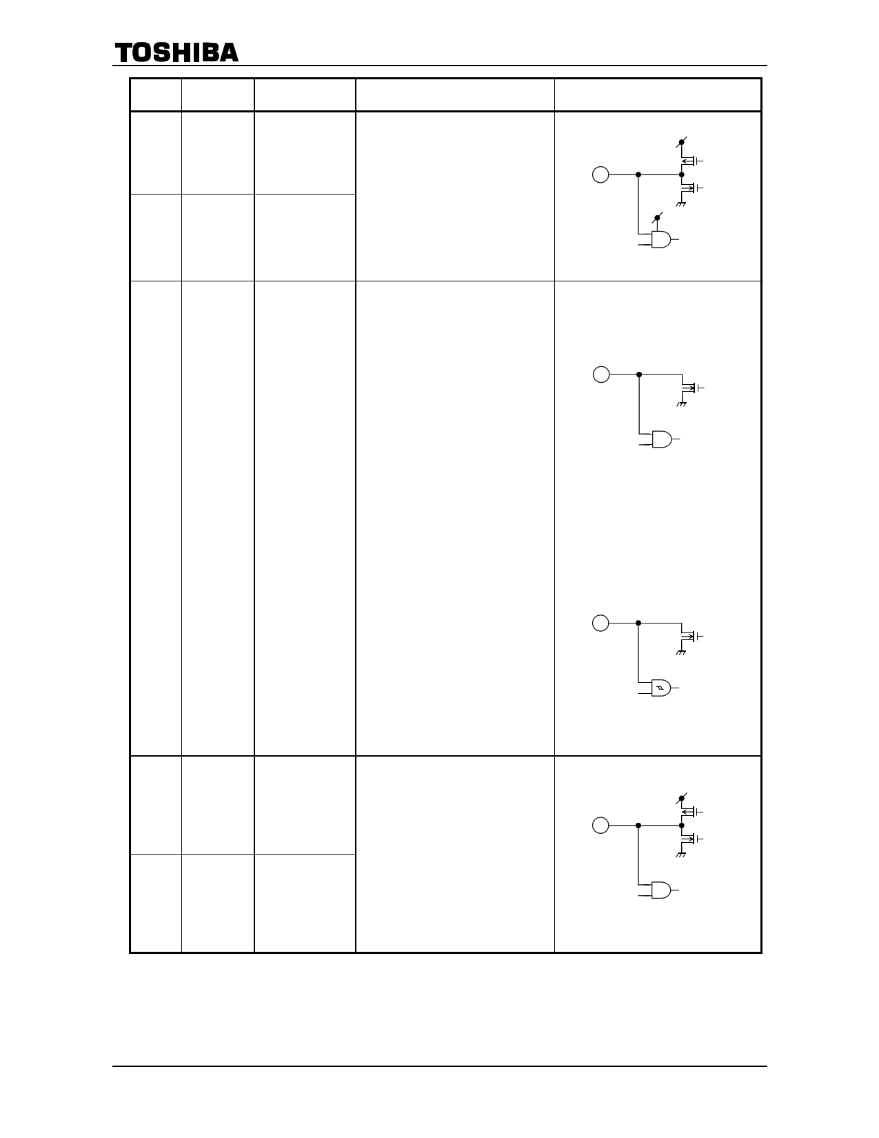
50~52 P2-0~P2-2 I/O port 2
I/O port 2
53 P2-3/PSC /Prescaler
/PSC output
The input and output of these 4-bit I/O
ports can be programmed in 1-bit units.
The P2-3 pin is also used as a PLL
prescaler PSC signal output pin. A PLL
can be configured using an external
prescaler. In such a case, set the pin to
I/O port output.
VLCD
VDD
Input
instruction
P3-0
P3-1/SI
42~45 P3-2/SO
P3-3/SCK
4-bit I/O ports, allowing input and output
to be programmed in 1-bit units. The
I/O ports are N-ch open drain.
Up to 3.6 V can be input. Even at low
voltage, N-ch high output current (2 mA
typ.) can be obtained.
These pins also function as serial
interface circuit (SIO) input/output pins.
I/O port 3
/Serial data input
There are two types of serial interface
circuit: SIO1 allows 4 or 8-bit
input/output and SIO2 allows 26-bit
serial data input. SIO1 inputs data of SI
pin serially with the edge of the clock of
SCK pin, and outputs it to SO pin.
/Serial data output
Internal (SCK = 37.5 kHz), external, or
rising/falling shift can be selected as the
clock (SCK) for serial operation. The
SO pin can be switched to serial input
(SI), facilitating LSI control and
communication between controllers.
/Serial clock I/O
Setting “1” in the SIO2 bit sets the SCK
pin to the SIO2 clock input and the
SI/SO pin to SIO2 data input. A
synchronization circuit is built-in for
SIO2.
When SIO interrupts are enabled, an
interrupt is generated after SIO
execution or by SIO2 operating clock
input and the program jumps to address
4.
All SIO inputs use built-in Schmitt
circuits.
SIO and all controls are programmable.
28
P4-0/BUZR
I/O port 4
/Buzzer output
29~31 P4-1~P4-3 I/O port 4
4-bit I/O ports, allowing input and output
to be programmed in 1-bit units.
The P4-0 pin is also used for buzzer
output.
The buzzer output can select 8 kinds of
0.625 to 3-kHz frequencies with 4
modes: continuous output, single-shot
output, 10 Hz intermittent output, and
10 Hz intermittent at 1 Hz intervals
output.
SIO, buzzer, and all associated controls
can be programmed.
Input
instruction (P3-0)
Input instruction + SIOon
(P3-1~P3-3)
VDD
Input
instruction
5 2006-03-02
5 Page 
TC9329AFAG/AFCG
Description of Operations
○ CPU
The CPU consists of a program counter, a stack register, an ALU, a program memory, a data memory, a
G-register, a data register, a DAL address register, a carry F/F, a judgment circuit, and an interruption
circuit.
1. Program Counter (PC)
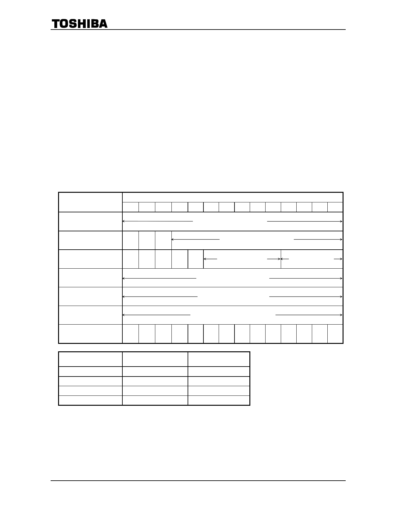
The program counter consists of a 14-bit binary up-counter and addresses the program memory (ROM).
The counter is cleared when the system is reset and the programs start from the 0 address.
Under normal conditions, the counter is increased in increments of one whenever an instruction is
executed, but the address specified in the instruction operand is loaded when a JUMP instruction or CALL
instruction is executed.
Also, when an instruction that is equipped with the skip function (AIS, SLTI, TMT, RNS instructions,
etc.) is executed, and the result of this includes a skip condition, the program counter is increased in
increments of two and the subsequent instruction is skipped. Furthermore, if interruption is received, the
vector address corresponding to each interruption is loaded.
Note: Addresses 0000H-0FFFH are reserved for the program memory. For this reason, access to addresses
outside this range is prohibited.
Instruction
JUMP ADDR1
Contens of Program Counter (PC)
PC13 PC12 PC11 PC10 PC9 PC8 PC7 PC6 PC5 PC4 PC3 PC2 PC1 PC0
Operand of instruction (ADDR1)
JUMP ADDR2
Power on reset
RESET by reset pin
DAL (DA)
(DAL bit = 1)
RN, RNS, RNI
At the time of an
interruption reception
Power on reset
RESET by reset pin
000
0 0 0 00
Operand of instruction (ADDR2)
Operand of
instruction (ADDR3)
Contents of general
register (r)
DAL address register (DA)
Contents of stack register
Vector address of each interruption
0 0 0 0 0000000000
Priority
1
2
3
4
Interruption Factor
INTR1 pin
INTR2 pin
Serial inter face
Timer counter
Vector Address
0001H
0002H
0003H
0004H
2. Stack Register
A register consisting of 8 × 14 bits which stores the contents of the program counter +1 (the return
address) when a sub-routine call instruction is executed. The contents of the stack register are loaded into
the program counter when the return instruction (RN, RNS, RNI instruction) is executed.
There are eight stack levels available and nesting occurs with both levels.
11 2006-03-02
11 Page | ||
| Páginas | Total 30 Páginas | |
| PDF Descargar | [ Datasheet TC9329AFCG.PDF ] | |
Hoja de datos destacado
| Número de pieza | Descripción | Fabricantes |
| TC9329AFCG | Portable Audio DTS Controller | Toshiba |
| Número de pieza | Descripción | Fabricantes |
| SLA6805M | High Voltage 3 phase Motor Driver IC. |
Sanken |
| SDC1742 | 12- and 14-Bit Hybrid Synchro / Resolver-to-Digital Converters. |
Analog Devices |
|
DataSheet.es es una pagina web que funciona como un repositorio de manuales o hoja de datos de muchos de los productos más populares, |
| DataSheet.es | 2020 | Privacy Policy | Contacto | Buscar |
