|
|
|
PDF CH7002D Data sheet ( Hoja de datos )
| Número de pieza | CH7002D | |
| Descripción | Scalable VGA to NTSC/PAL Encoder | |
| Fabricantes | ETC | |
| Logotipo | ||
Hay una vista previa y un enlace de descarga de CH7002D (archivo pdf) en la parte inferior de esta página. Total 36 Páginas | ||
|
No Preview Available !
CHRONTEL
CH7002D
Preliminary
Scalable VGA to NTSC/PAL Encoder
Features
• Fully integrated solution for PC to TV display
• TrueScale TM rendering engine supports underscan
operation for both 640x480 or 800x600 inputs †
• Advanced 3-line digital flicker filtering with
programmable algorithm selections †
• Fully programmable through I2C port or hardware
(pin-based) controls
• Wide range of VGA software drivers for full
synchronization and image positioning
• Auto-detection of TV presence
• Programmable power management features three
power-down modes
• Supports both NTSC and PAL (B, D, G, H, or I) TV
formats onto both composite and S-Video
• Triple 8-bit ADC inputs and triple 8-bit DAC outputs
• On-chip reference generation and loop filter
• Offered in 44-pin PLCC package
General Description
Chrontel’s CH7002 VGA to NTSC/PAL encoder is a stand-
alone integrated circuit which provides a PC 99 compliant
solution for TV output. It accepts RGB analog inputs directly
from VGA controllers and converts them directly into NTSC
or PAL TV format, with simultaneous composite and
S-Video outputs.
This circuit integrates a digital NTSC/PAL encoder with 8-
bit ADC and DAC interfaces, a 3-line vertical filter, and low-
jitter phase-locked loop to create outstanding quality video.
Through Chrontel’s TrueScale TM rendering technology, the
CH7002 supports full vertical and horizontal underscan
operation from either 640x480 or 800x600 input to either
NTSC or PAL outputs.
A high level of performance along with full programmability
makes the CH7002 ideal for system-level PC or Web
browser solutions. All features are software programmable,
through a standard I2C port, to enable fully integrated system
solutions by using a TV as the primary display device.
† Patent number 5,781,241
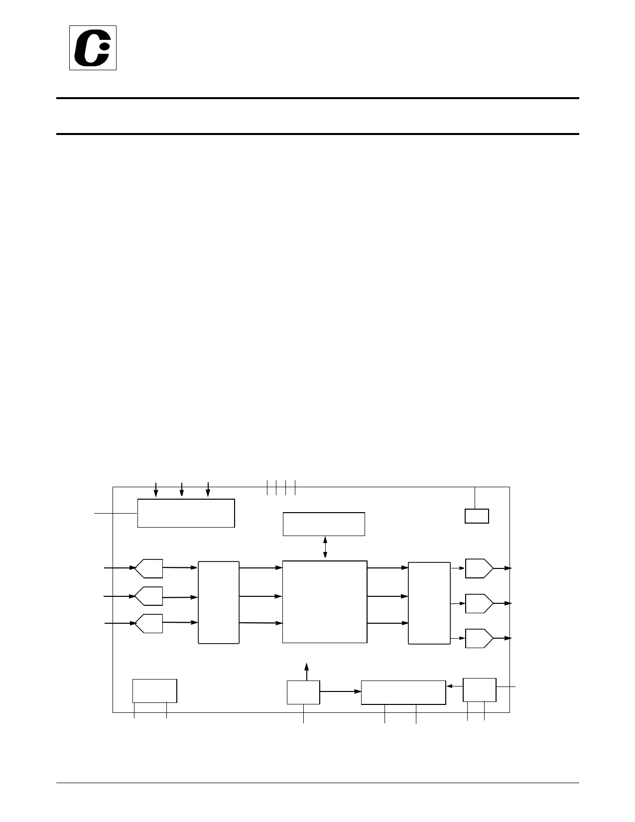
PMODE
SD SC ADDR
I2C REGISTER & CONTROL
BLOCK
LINE
MEMORY
RSET
RSET
RR
ADC
Y
LINE RENDERING ENGINE
G
G COLOR
U
ADC
SPACE
-SCALING
CONVERTER
-DEFLICKERING
BB
V -SCAN CONVERSION
ADC
SYSTEM CLOCK
Y
U DIGITAL
NTSC/PAL
ENCODER
V & FILTER
DAC
DAC
DAC
VREF
PLL
TIMING & SYNC GENERATOR
OSC
VREF1 VREF2
XCLK
HV
Figure 1: Functional Block Diagram
XI XO
Y
CVBS
C
CLKOUT
201-0000-029 Rev 6.1, 8/2/99
1
1 page 
CHRONTEL
CH7002D
Table 1. Pin Description (continued)
44-Pin
PLCC
36
38
41
43
19, 20
Type
In
In
In
In
NC
Symbol
Description
ADDR/FF0
PMODE
VREF2
VREF1
NC
I2C Address Select/Flicker Filter (bit 0)(internal pull-up)
The function of this dual use pin is determined by the state of the PMODE pin.
When the PMODE pin is kept high (default), this pin becomes ADDR or I2C
Address Select, which corresponds to bits 1 and 0 of the I2C device address
(see the I2C Control Port Operation section for details), creating an address
selection as follows:
ADDR I2C Address Selected
1 1110101 = 75H = 117
0 1110110 = 76H = 118
When the PMODE pin is pulled low, this pin becomes FF0 or Flicker Filter
select, the function of which corresponds to bit 0 of the Flicker Filter register,
which selects between the following:
FF0 Flicker Filter Mode
0 0:1:0 No filtering
1 1:2:1 Moderate filtering (default)
This pin-programming is “mux-ed” with the Flicker Filter register (bit 0). All
related modes are described under the Registers and Programming section.
Programming Mode (internal pull-up)
The PMODE pin selects between the two alternative programming modes for
the CH7002, which in turn alters the function of five additional pins
(RESET/DM0, SD/DM1, SC/DM2, XCLK/SD3, and ADDR/FF0). When
PMODE is kept high (default), the chip is placed in I2C programming mode.
When PMODE is pulled low, the chip is placed in direct pin programming
mode.
Internal Voltage Reference
VREF2 provides a typical 2.5V reference that is used as an internal bias to
the ADCs. A 0.1 µF decoupling capacitor should be connected between
VREF2 and ground.
ADC Voltage Reference Input / Output
VREF1 provides a typical 1.235V reference that sets the RGB input full scale
at 0.75V. A 0.1 µF decoupling capacitor should be connected between
VREF1 and ground. VREF1 may also be forced by external reference, where
(VFS is the full scale input voltage):
VFS ~ VREF1 * 0.75/1.235
No Connect
Note: For complete information concerning external signal connections, terminations, and system design considerations,
refer to the Application Information section.
201-0000-029 Rev 6.1, 8/2/99
5
5 Page 
CHRONTEL
CH7002D
0
-1
-2
-3
-4
dB -5
-6
-7
-8
-9
-10
0 1 2 3 4 56
Freq (MHz)
Figure 6: Luminance Frequency Response - Detailed View
Y_SV0
Y_SV1
Y_SV2
Y_CVO
Y_CV1
0
-10
-20
dB
-30
-40
01
23 4 5 6
7 8 9 10 11 12
Y_SV0
Y_SV1
Y_SV2
Y_CVO
Y_CV1
Freq (MHz)
Figure 7: Luminance Frequency Response - Full View
Notes:
1 The curves shown are valid for operating modes 2 and 6. Mode 0 frequency values are 20% higher, mode 1
and 3 frequency values are 12% higher, and mode 4 frequency values are 1% lower, due to changes in clock
frequencies.
2 The Y_SV1 and Y_CV0 responses are identical; therefore the curves lie on top of each other.
201-0000-029 Rev 6.1, 8/2/99
11
11 Page | ||
| Páginas | Total 36 Páginas | |
| PDF Descargar | [ Datasheet CH7002D.PDF ] | |
Hoja de datos destacado
| Número de pieza | Descripción | Fabricantes |
| CH7002D | Scalable VGA to NTSC/PAL Encoder | ETC |
| CH7002D-V | Scalable VGA to NTSC/PAL Encoder | ETC |
| Número de pieza | Descripción | Fabricantes |
| SLA6805M | High Voltage 3 phase Motor Driver IC. |
Sanken |
| SDC1742 | 12- and 14-Bit Hybrid Synchro / Resolver-to-Digital Converters. |
Analog Devices |
|
DataSheet.es es una pagina web que funciona como un repositorio de manuales o hoja de datos de muchos de los productos más populares, |
| DataSheet.es | 2020 | Privacy Policy | Contacto | Buscar |