|
|
|
PDF HMC988LP3E Data sheet ( Hoja de datos )
| Número de pieza | HMC988LP3E | |
| Descripción | PROGRAMMABLE CLOCK DIVIDER AND DELAY | |
| Fabricantes | Hittite Microwave Corporation | |
| Logotipo | ||
Hay una vista previa y un enlace de descarga de HMC988LP3E (archivo pdf) en la parte inferior de esta página. Total 22 Páginas | ||
|
No Preview Available !
HMC988LP3E
v04.1014
PROGRAMMABLE CLOCK DIVIDER AND DELAY
DC - 4 GHz
Typical Applications
The HMC988LP3E is ideal for:
• Basestation Digital Pre-Distortion Paths(DPD)
• High Performance Automated Test
Equipment(ATE)
• Backplane clock skew management
• Phase Coherence of multiple clock paths
• Clock Delay management to improve setup &
hold time margins
• PCB signal flight time offset circuits
• Track and hold circuits for ADC/DACs
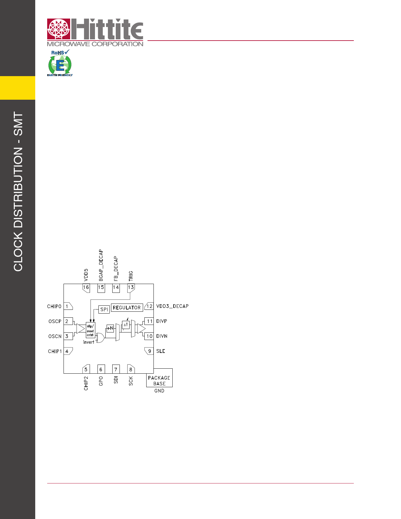
Functional Diagram
Features
DC - 4 GHz
-170 dBc/Hz floor @ 100 MHz output
-164 dBc/Hz floor @ 2 GHz output
Integrated Jitter 35 fsRMS@ 100 MHz output
13 fsRMS(calculated) @ 2 GHz output
Adjustable output phase with soft/hard reset sync
Adjustable output delay in 60 steps of 20 ps
Flexible Input Interface:
LVPECL,LVDS,CML,CMOS Compatible
AC or DC Coupling
On - Chip Termination 50 Ω (100 Ω Differential)
Output Driver (LVPECL):
800 mVpp LVPECL into 50 Ω Single-Ended (+3
dBm Fo)
Up to 8 addressable dividers per SPI bus
3.3 V operation or 5 V operation with Optional on-
chip regulator for best performance
3 x 3 QFN Leadless SMT Package
General Description
The HMC988LP3E is a an ultra low noise clock
divider capable of dividing by 1/2/4/8/16/32. It is a
versatile device with additional functionality including
adjustable output phase, adjustable delay in 60 steps
of ~ 20 ps, a clock synchronization function, and a
clock invert option.
Housed in a compact 3x3 mm SMT QFN package, the
clock divider offers a high level of functionality. The
device works with 3.3 V supply or may be connected
to 5 V supply and utilize the optional on-chip regulator.
This on-chip regulator may be bypassed.
Up to 8 addressable HMC988LP3E devices can be
used together on the SPI bus.
The HMC988LP3E is ideally suited for data converter
applications with extremely low phase noise
requirements.
For price, delivery and to place orders: Hittite Microwave Corporation, 2 Elizabeth Drive, Chelmsford, MA 01824
1
Phone: 978-250-3343 Fax: 978-250-3373 Order On-line at www.hittite.com
Application Support: Phone: 978-250-3343 or [email protected]
1 page 
HMC988LP3E
v04.1014
PROGRAMMABLE CLOCK DIVIDER AND DELAY
DC - 4 GHz
Figure 7. S-Parameters-S22 [4]
0
-5
-10
-15
S22(Single-Ended)
S22(Differnetial)
-20
100000
1000000
FREQUENCY (KHz)
Figure 9. Input Sensitivity[5]
5E+06
200
180
160
140
Recommended Operating Region
120
100
80
60
40
20
0
01234
INPUT FREQUENCY (GHz)
Figure 11. Time Domain 1 GHz input,
500 MHz Output [7]
400
5
300
200
100
0
-100
-200
-300
-400
0 210 500
1000
1500 2000 2500
TIME (ps)
3000
3500
4000
Figure 8. S-Parameters-S11 [4]
0
-5
-10
-15
-20
-25
-30
-35 S11(Single-Ended)
S11(Differnetial)
-40
1E+5
1E+6
5E+6
FREQUENCY (KHz)
Figure 10. Supply Voltage vs input Voltage [6]
3.6
3.4
3.2
3
VOUT(Regulated)
VOUT(non regulated)
2.8
2.6
3 3.5 4 4.5 5 5.5
VIN (V)
[4] Measured with 200 Ω DC termination, 10 Ω series resistor in front, AC couple 1 nF 3.3 V
[5] Measured single-ended. 120 Ω DC termination, 3.3 V HMC988LP5E AC coupled to 50 Ω instrument(DSO8104B) with divider bypass. ESD diode
will start to turn on if maximum input power exceeds 12 dBm.
[6] On Chip regulator enable mode measured at PIN CAP_3V Vs regulator bypass mode
[7] Measured with 1 GHz 400 mVpp source as single ended input, HMC988LP3E div 2. Board delay 210 ps
For price, delivery and to place orders: Hittite Microwave Corporation, 2 Elizabeth Drive, Chelmsford, MA 01824
5
Phone: 978-250-3343 Fax: 978-250-3373 Order On-line at www.hittite.com
Application Support: Phone: 978-250-3343 or [email protected]
5 Page 
HMC988LP3E
v04.1014
PROGRAMMABLE CLOCK DIVIDER AND DELAY
DC - 4 GHz
Theory of Operation
In addition to HMC988LP3E excellent low noise performance, the device offers additional functionality including:
Modular Configuration
Synchronization Function
Adjustable Fine Delay
Adjustable Coarse Delay
Trigger Options
Optional On-Chip Regulator
GPO
Modular Configuration
The HMC988LP3E has been designed so that up to 8 devices can be placed on one SPI bus. The part has a 3-bit
addressable chip addresses (CHIP0 pin, CHIP1 pin, CHIP2 pin) so that each chip can be controlled individually. In
addition, HMC988LP3E has a broadcast mode which allows up to 8 HMC988LP3E devices to be simultaneously
controlled, or triggered. In Broadcast mode each HMC988LP3E device will listen to the same chip address, namely
“111.” Typical application of HMC988LP3E is shown in Figure 1.
Figure 1. Typical application of HMC988LP3E
For price, delivery and to place orders: Hittite Microwave Corporation, 2 Elizabeth Drive, Chelmsford, MA 01824
11
Phone: 978-250-3343 Fax: 978-250-3373 Order On-line at www.hittite.com
Application Support: Phone: 978-250-3343 or [email protected]
11 Page | ||
| Páginas | Total 22 Páginas | |
| PDF Descargar | [ Datasheet HMC988LP3E.PDF ] | |
Hoja de datos destacado
| Número de pieza | Descripción | Fabricantes |
| HMC988LP3E | PROGRAMMABLE CLOCK DIVIDER AND DELAY | Hittite Microwave Corporation |
| Número de pieza | Descripción | Fabricantes |
| SLA6805M | High Voltage 3 phase Motor Driver IC. |
Sanken |
| SDC1742 | 12- and 14-Bit Hybrid Synchro / Resolver-to-Digital Converters. |
Analog Devices |
|
DataSheet.es es una pagina web que funciona como un repositorio de manuales o hoja de datos de muchos de los productos más populares, |
| DataSheet.es | 2020 | Privacy Policy | Contacto | Buscar |