|
|
|
PDF ADuM240E Data sheet ( Hoja de datos )
| Número de pieza | ADuM240E | |
| Descripción | 5.0 kV rms Quad Digital Isolators | |
| Fabricantes | Analog Devices | |
| Logotipo | ||
Hay una vista previa y un enlace de descarga de ADuM240E (archivo pdf) en la parte inferior de esta página. Total 26 Páginas | ||
|
No Preview Available !
5.0 kV rms Quad Digital Isolators
Data Sheet ADuM240D/ADuM240E/ADuM241D/ADuM241E/ADuM242D/ADuM242E
FEATURES
High common-mode transient immunity: 100 kV/μs
High robustness to radiated and conducted noise
Low propagation delay
13 ns maximum for 5 V operation
15 ns maximum for 1.8 V operation
150 Mbps maximum guaranteed data rate
Safety and regulatory approvals (pending)
UL recognition: 5000 V rms for 1 minute per UL 1577
CSA Component Acceptance Notice 5A
VDE certificate of conformity
DIN V VDE V 0884-10 (VDE V 0884-10):2006-12
VIORM = 849 V peak
8000 V peak reinforced surge isolation voltage
CQC certification per GB4943.1-2011
Backward compatibility
ADuM240E1/ADuM241E1/ADuM242E1 pin compatible
with ADuM2400/ADuM2401/ADuM2402
Low dynamic power consumption
1.8 V to 5 V level translation
High temperature operation: 125°C
Fail-safe high or low options
16-lead, RoHS compliant, SOIC package
Qualified for automotive applications
APPLICATIONS
General-purpose multichannel isolation
Serial peripheral interface (SPI)/data converter isolation
Industrial field bus isolation
GENERAL DESCRIPTION
The ADuM240D/ADuM240E/ADuM241D/ADuM241E/
ADuM242D/ADuM242E1 are quad-channel digital isolators
based on Analog Devices, Inc., iCoupler® technology. Combining
high speed, complementary metal-oxide semiconductor (CMOS)
and monolithic air core transformer technology, these isolation
components provide outstanding performance characteristics
superior to alternatives such as optocoupler devices and other
integrated couplers. The maximum propagation delay is 13 ns
with a pulse width distortion of less than 3 ns at 5 V operation.
Channel matching is tight at 3.0 ns maximum.
The ADuM240D/ADuM240E/ADuM241D/ADuM241E/
ADuM242D/ADuM242E data channels are independent and
are available in a variety of configurations with a withstand
voltage rating of 5.0 kV rms (see the Ordering Guide). The
devices operate with the supply voltage on either side ranging
from 1.8 V to 5 V, providing compatibility with lower voltage
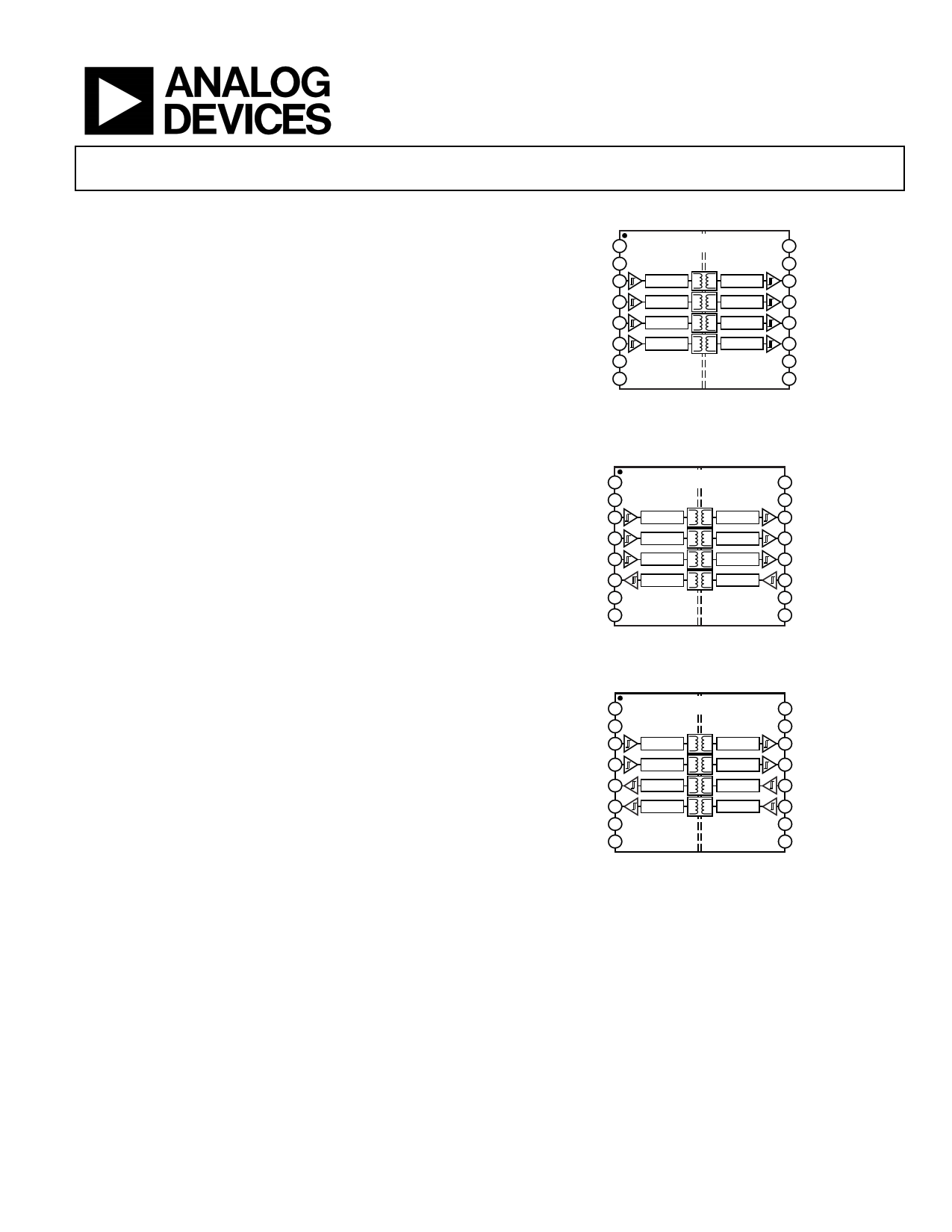
FUNCTIONAL BLOCK DIAGRAMS
VDD1 1 ADuM240D/ADuM240E 16 VDD2
GND1 2
VIA 3
ENCODE
DECODE
15 GND2
14 VOA
VIB 4
ENCODE
DECODE
13 VOB
VIC 5
ENCODE
DECODE
12 VOC
VID 6
ENCODE
DECODE
11 VOD
DISABLE1/NIC 7
GND1 8
10 NIC/VE2
9 GND2
NOTES
1. NIC = NO INTERNAL CONNECTION. LEAVE THIS PIN FLOATING.
2. PIN 7 IS DISABLE1 AND PIN 10 IS NIC FOR THE ADuM240D, AND
PIN 7 IS NIC AND PIN 10 IS VE2 FOR THE ADuM240E.
Figure 1. ADuM240D/ADuM240E Functional Block Diagram
VDD1 1 ADuM241D/ADuM241E 16 VDD2
GND1 2
VIA 3
ENCODE
DECODE
15 GND2
14 VOA
VIB 4
ENCODE
DECODE
13 VOB
VIC 5
ENCODE
DECODE
12 VOC
VOD 6
DECODE
ENCODE
11 VID
DISABLE1/VE1 7
GND1 8
10 DISABLE2/VE2
9 GND2
NOTES
1. PIN 7 IS DISABLE1 AND PIN 10 IS DISABLE2 FOR THE ADuM241D,
AND PIN 7 IS VE1 AND PIN 10 IS VE2 FOR THE ADuM241E.
Figure 2. ADuM241D/ADuM241E Functional Block Diagram
VDD1 1
GND1 2
VIA 3
ADuM242D/ADuM242E
ENCODE
DECODE
16 VDD2
15 GND2
14 VOA
VIB 4
ENCODE
DECODE
13 VOB
VOC 5
DECODE
ENCODE
12 VIC
VOD 6
DECODE
ENCODE
11 VID
DISABLE1/VE1 7
GND1 8
10 DISABLE2/VE2
9 GND2
NOTES
1. PIN 7 IS DISABLE1 AND PIN 10 IS DISABLE2 FOR THE ADuM242D,
AND PIN 7 IS VE1 AND PIN 10 IS VE2 FOR THE ADuM242E.
Figure 3. ADuM242D/ADuM242E Functional Block Diagram
systems as well as enabling voltage translation functionality
across the isolation barrier.
Unlike other optocoupler alternatives, dc correctness is ensured in
the absence of input logic transitions. Two different fail-safe options
are available by which the outputs transition to a predetermined
state when the input power supply is not applied or the inputs are
disabled. The ADuM240E1/ADuM241E1/ ADuM242E1 are pin
compatible with the ADuM2400/ ADuM2401/ADuM2402.
1 Protected by U.S. Patents 5,952,849; 6,873,065; 6,903,578; and 7,075,329. Other patents are pending.
Rev. A
Document Feedback
Information furnished by Analog Devices is believed to be accurate and reliable. However, no
responsibility is assumed by Analog Devices for its use, nor for any infringements of patents or other
rights of third parties that may result from its use. Specifications subject to change without notice. No
license is granted by implication or otherwise under any patent or patent rights of Analog Devices.
Trademarksandregisteredtrademarksarethepropertyoftheirrespectiveowners.
One Technology Way, P.O. Box 9106, Norwood, MA 02062-9106, U.S.A.
Tel: 781.329.4700 ©2015–2016 Analog Devices, Inc. All rights reserved.
Technical Support
www.analog.com
1 page 
Data Sheet ADuM240D/ADuM240E/ADuM241D/ADuM241E/ADuM242D/ADuM242E
ELECTRICAL CHARACTERISTICS—3.3 V OPERATION
All typical specifications are at TA = 25°C, VDD1 = VDD2 = 3.3 V. Minimum/maximum specifications apply over the entire recommended
operation range: 3.0 V ≤ VDD1 ≤ 3.6 V, 3.0 V ≤ VDD2 ≤ 3.6 V, and −40°C ≤ TA ≤ +125°C, unless otherwise noted. Switching specifications
are tested with CL = 15 pF and CMOS signal levels, unless otherwise noted. Supply currents are specified with 50% duty cycle signals.
Table 3.
Parameter
SWITCHING SPECIFICATIONS
Pulse Width
Data Rate1
Propagation Delay
Pulse Width Distortion
Change vs. Temperature
Propagation Delay Skew
Channel Matching
Codirectional
Opposing Direction
Jitter
DC SPECIFICATIONS
Input Threshold Voltage
Logic High
Logic Low
Output Voltage
Logic High
Logic Low
Input Current per Channel
VE2 Enable Input Pull-Up Current
DISABLE1 Input Pull-Down Current
Tristate Output Current per Channel
Quiescent Supply Current
ADuM240D/ADuM240E
ADuM241D/ADuM241E
ADuM242D/ADuM242E
Dynamic Supply Current
Dynamic Input
Dynamic Output
Symbol Min
Typ Max Unit
Test Conditions/Comments
PW 6.6
ns Within PWD limit
150
Mbps
Within PWD limit
tPHL, tPLH 4.8
6.8 14
ns
50% input to 50% output
PWD
0.7 3 ns |tPLH − tPHL|
1.5 ps/°C
tPSK
7.5 ns
Between any two units at the same
temperature, voltage, and load
tPSKCD
tPSKOD
0.7 3.0
0.7 3.0
580
120
ns
ns
ps p-p
ps rms
See the Jitter Measurement section
See the Jitter Measurement section
VIH 0.7 × VDDx
VIL
V
0.3 × VDDx V
VOH VDDx − 0.1 VDDx
VDDx − 0.4 VDDx − 0.2
VOL 0.0 0.1
0.2 0.4
II
−10
+0.01
+10
IPU −10 −3
IPD 9 15
IOZ
−10
+0.01
+10
V
V
V
V
μA
μA
μA
μA
IOx2 = −20 μA, VIx = VIxH3
IOx2 = −2 mA, VIx = VIxH3
IOx2 = 20 μA, VIx = VIxL4
IOx2 = 2 mA, VIx = VIxL4
0 V ≤ VIx ≤ VDDx
VE2 = 0 V
DISABLE1 = VDDx
0 V ≤ VOx ≤ VDDx
IDD1 (Q)
IDD2 (Q)
IDD1 (Q)
IDD2 (Q)
IDD1 (Q)
IDD2 (Q)
IDD1 (Q)
IDD2 (Q)
IDD1 (Q)
IDD2 (Q)
IDD1 (Q)
IDD2 (Q)
IDDI (D)
IDDO (D)
1.2 2.12 mA
2.0 2.68 mA
12.0 19.6 mA
2.0 2.8 mA
VI5 = 0 (E0, D0), 1 (E1, D1)6
VI5 = 0 (E0, D0), 1 (E1, D1)6
VI5 = 1 (E0, D0), 0 (E1, D1)6
VI5 = 1 (E0, D0), 0 (E1, D1)6
1.5 2.36 mA
1.8 2.52 mA
9.8 16.7 mA
5.7 9.7 mA
VI5 = 0 (E0, D0), 1 (E1, D1)6
VI5 = 0 (E0, D0), 1 (E1, D1)6
VI5 = 1 (E0, D0), 0 (E1, D1)6
VI5 = 1 (E0, D0), 0 (E1, D1)6
1.6 2.4 mA
1.6 2.4 mA
7.0 11.2 mA
7.0 11.2 mA
VI5 = 0 (E0, D0), 1 (E1, D1)6
VI5 = 0 (E0, D0), 1 (E1, D1)6
VI5 = 1 (E0, D0), 0 (E1, D1)6
VI5 = 1 (E0, D0), 0 (E1, D1)6
0.01 mA/Mbps Inputs switching, 50% duty cycle
0.01 mA/Mbps Inputs switching, 50% duty cycle
Rev. A | Page 5 of 26
5 Page 
Data Sheet ADuM240D/ADuM240E/ADuM241D/ADuM241E/ADuM242D/ADuM242E
INSULATION AND SAFETY RELATED SPECIFICATIONS
For additional information, see www.analog.com/icouplersafety.
Table 9. RW-16 Wide Body [SOIC_W] Package
Parameter
Rated Dielectric Insulation Voltage
Minimum External Air Gap (Clearance)
Symbol
L (I01)
Minimum External Tracking (Creepage)
L (I02)
Minimum Clearance in the Plane of the Printed
Circuit Board (PCB Clearance)
L (PCB)
Minimum Internal Gap (Internal Clearance)
Tracking Resistance (Comparative Tracking Index)
Material Group
CTI
Value
5000
7.8
7.8
8.1
25.5
>400
II
Unit
V rms
mm min
mm min
mm min
μm min
V
Test Conditions/Comments
1-minute duration
Measured from input terminals to output terminals,
shortest distance through air
Measured from input terminals to output terminals,
shortest distance path along body
Measured from input terminals to output terminals,
shortest distance through air, line of sight, in the PCB
mounting plane
Insulation distance through insulation
DIN IEC 112/VDE 0303 Part 1
Material Group (DIN VDE 0110, 1/89, Table 1)
Table 10. RI-16 -2 Wide Body Increased Creepage [SOIC_IC] Package
Parameter
Symbol Value Unit
Rated Dielectric Insulation Voltage
5000 V rms
Minimum External Air Gap (Clearance)
L (I01) 8.3
mm min
Minimum External Tracking (Creepage)
L (I02) 8.3
mm min
Minimum Clearance in the Plane of the Printed
Circuit Board (PCB Clearance)
L (PCB) 8.3
mm min
Minimum Internal Gap (Internal Clearance)
Tracking Resistance (Comparative Tracking Index)
Material Group
CTI
25.5
>400
II
μm min
V
Test Conditions/Comments
1-minute duration
Measured from input terminals to output terminals,
shortest distance through air
Measured from input terminals to output terminals,
shortest distance path along body
Measured from input terminals to output terminals,
shortest distance through air, line of sight, in the PCB
mounting plane
Insulation distance through insulation
DIN IEC 112/VDE 0303 Part 1
Material Group (DIN VDE 0110, 1/89, Table 1)
PACKAGE CHARACTERISTICS
Table 11.
Parameter
Resistance (Input to Output)1
Capacitance (Input to Output)1
Input Capacitance2
IC Junction to Ambient Thermal Resistance
Symbol Min Typ Max Unit Test Conditions/Comments
RI-O 1013 Ω
CI-O 2.2 pF f = 1 MHz
CI 4.0 pF
θJA 45 °C/W Thermocouple located at center of package underside
1 The device is considered a 2-terminal device: Pin 1 through Pin 8 are shorted together, and Pin 9 through Pin 16 are shorted together.
2 Input capacitance is from any input data pin to ground.
Rev. A | Page 11 of 26
11 Page | ||
| Páginas | Total 26 Páginas | |
| PDF Descargar | [ Datasheet ADuM240E.PDF ] | |
Hoja de datos destacado
| Número de pieza | Descripción | Fabricantes |
| ADUM2400 | (ADUM2400 - ADUM2402) Quad-Channel Digital Isolators | Analog Devices |
| ADUM2401 | (ADUM2400 - ADUM2402) Quad-Channel Digital Isolators | Analog Devices |
| ADUM2402 | (ADUM2400 - ADUM2402) Quad-Channel Digital Isolators | Analog Devices |
| ADuM240D | 5.0 kV rms Quad Digital Isolators | Analog Devices |
| Número de pieza | Descripción | Fabricantes |
| SLA6805M | High Voltage 3 phase Motor Driver IC. |
Sanken |
| SDC1742 | 12- and 14-Bit Hybrid Synchro / Resolver-to-Digital Converters. |
Analog Devices |
|
DataSheet.es es una pagina web que funciona como un repositorio de manuales o hoja de datos de muchos de los productos más populares, |
| DataSheet.es | 2020 | Privacy Policy | Contacto | Buscar |