|
|
|
PDF AMD533CE Data sheet ( Hoja de datos )
| Número de pieza | AMD533CE | |
| Descripción | N & P-Channel MOSFET | |
| Fabricantes | Analog Power | |
| Logotipo | ||
Hay una vista previa y un enlace de descarga de AMD533CE (archivo pdf) en la parte inferior de esta página. Total 7 Páginas | ||
|
No Preview Available !
Analog Power
AMD533CE
P & N-Channel 30-V (D-S) MOSFET
These miniature surface mount MOSFETs utilize a
high cell density trench process to provide low
rDS(on) and to ensure minimal power loss and heat
dissipation. Typical applications are DC-DC
converters and power management in portable and
battery-powered products such as computers,
printers, PCMCIA cards, cellular and cordless
telephones.
PRODUCT SUMMARY
VDS (V)
rDS(on) m(Ω)
30 45 @VGS = 4.5V
35 @VGS =10V
-30 70 @VGS =-4.5V
52 @VGS = -10V
ID (A)
29
36
-20
-26
• Low rDS(on) provides higher efficiency and
extends battery life
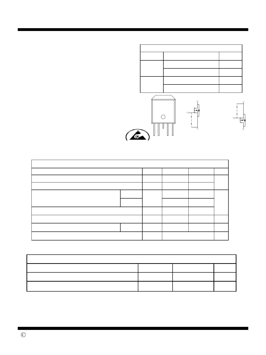
D1
S
2
• Low thermal impedance copper leadframe
DPAK saves board space
G
1
G
2
• Fast switching speed
• High performance trench technology
S1 G1 D S2 G2
S
1
N-Channel MOSFET
D2
P-Channel MOSFET
ESD Protected
2000V
ABSOLUTE MAXIMUMRATINGS (TA = 25 oCUNLESS OTHERWISENOTED)
Parameter
Symbol N-Channel P-Channel Units
Drain-Source Voltage
Gate-Source Voltage
Continuous Drain Currenta
Pulsed Drain Currentb
VDS
VGS
TA=25oC
TA=70oC
ID
IDM
30
±20
-30
±20
V
36 -26
30 -21 A
40 -40
Continuous Source Current (Diode Conduction)a
IS
30 -30 A
Power Dissipationa
TA=25oC PD
Operating Junction and Storage Temperature Range TJ, Tstg
50 50
-55 to 175
W
oC
THERMAL RESISTANCE RATINGS
Parameter
Symbol
Maximum Junction-to-Ambienta
RθJA
Maximum Junction-to-Case
RθJC
Maximum
50
3.0
Units
oC/W
oC/W
Notes
a. Surface Mounted on 1” x 1” FR4 Board.
b. Pulse width limited by maximum junction temperature
PRELIMINARY
1 Publication Order Number:
DS-AMD533CE_D
1 page 
Analog Power
AMD533CE
Typical Electrical Characteristics (P-Channel)
30
VGS = -10V
-6.0V
-5.0V
20
-4.0V
10
-3.0V
0
0123456
-VDS, DRAIN TO SOURCE VOLTAGE (V)
Figure 1. On-Region Characteristics
2
1.8
1.6
-4.5V
1.4
-6.0V
1.2
-10V
1
0.8
0
6 12 18 24
-ID, DRAIN CURRENT (A)
30
Figure 3. On Resistance Vs Vgs Voltage
10
ID = -5.7A
8
6
-15V
4
2
0
02468
Qg, GATE CHARGE (nC)
Figure 5. Gate Charge Characteristics
10
15
VDS = -5V
12
9
TA = -55oC
25oC
125oC
6
3
0
1 1.5 2 2.5 3 3.5 4 4.5
-VGS, GATE TO SOURCE VOLTAGE (V)
Figure 2. Body Diode Forward Voltage Variation
with Source Current and Temperature
800
700
f = 1 MHz
VGS = 0 V
600 CISS
500
400
300
200 COSS
100
CRSS
0
0
5
10 15 20 25
-VDS, DRAIN TO SOURCE VOLTAGE (V)
30
Figure 4. Capacitance Characteristics
1.6
VGS = 10V
1.4 ID = 5.7A
1.2
1.0
0.8
0.6
-50 -25 0 25 50 75 100 125 150
TJ Juncation Temperature (C)
Figure 6. On-Resistance Variation with Temperature
PRELIMINARY
5 Publication Order Number:
DS-AMD533CE_D
5 Page | ||
| Páginas | Total 7 Páginas | |
| PDF Descargar | [ Datasheet AMD533CE.PDF ] | |
Hoja de datos destacado
| Número de pieza | Descripción | Fabricantes |
| AMD533CE | N & P-Channel MOSFET | Analog Power |
| Número de pieza | Descripción | Fabricantes |
| SLA6805M | High Voltage 3 phase Motor Driver IC. |
Sanken |
| SDC1742 | 12- and 14-Bit Hybrid Synchro / Resolver-to-Digital Converters. |
Analog Devices |
|
DataSheet.es es una pagina web que funciona como un repositorio de manuales o hoja de datos de muchos de los productos más populares, |
| DataSheet.es | 2020 | Privacy Policy | Contacto | Buscar |