|
|
|
PDF GS8182S18D Data sheet ( Hoja de datos )
| Número de pieza | GS8182S18D | |
| Descripción | 18Mb Burst of 2 DDR SigmaSIO-II SRAM | |
| Fabricantes | GSI Technology | |
| Logotipo | ||
Hay una vista previa y un enlace de descarga de GS8182S18D (archivo pdf) en la parte inferior de esta página. Total 30 Páginas | ||
|
No Preview Available !
GS8182S18D-267/250/200/167
165-Bump BGA
Commercial Temp
Industrial Temp
18Mb Burst of 2
DDR SigmaSIO-II SRAM
267 MHz–167 MHz
1.8 V VDD
1.8 V and 1.5 V I/O
Features
• Simultaneous Read and Write SigmaQuad™ Interface
• JEDEC-standard pinout and package
• Dual Double Data Rate interface
• Byte Write controls sampled at data-in time
• DLL circuitry for wide output data valid window and future
frequency scaling
• Burst of 2 Read and Write
• 1.8 V +150/–100 mV core power supply
• 1.5 V or 1.8 V HSTL Interface
• Pipelined read operation
• Fully coherent read and write pipelines
• ZQ mode pin for programmable output drive strength
• IEEE 1149.1 JTAG-compliant Boundary Scan
• 165-bump, 13 mm x 15 mm, 1 mm bump pitch BGA package
• RoHS-compliant 165-bump BGA package available
• Pin-compatible with future 36Mb, 72Mb, and 144Mb devices
SigmaRAM™ Family Overview
GS8182S18 are built in compliance with the SigmaSIO-II
SRAM pinout standard for Separate I/O synchronous SRAMs.
They are 18,874,368-bit (18Mb) SRAMs. These are the first in
a family of wide, very low voltage HSTL I/O SRAMs designed
to operate at the speeds needed to implement economical high
performance networking systems.
Clocking and Addressing Schemes
A Burst of 2 SigmaSIO-II SRAM is a synchronous device. It
employs dual input register clock inputs, K and K. The device
also allows the user to manipulate the output register clock
input quasi independently with dual output register clock
inputs, C and C. If the C clocks are tied high, the K clocks are
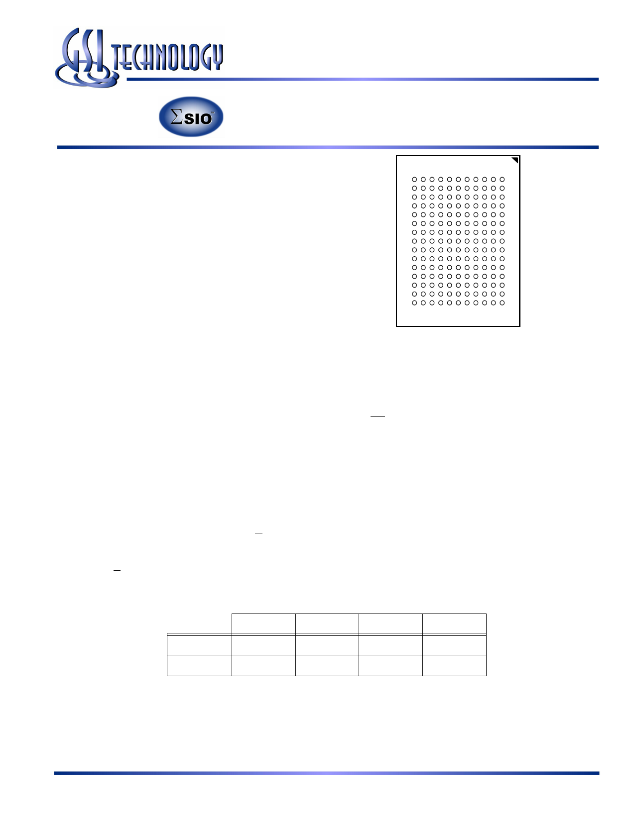
Bottom View
165-Bump, 13 mm x 15 mm BGA
1 mm Bump Pitch, 11 x 15 Bump Array
JEDEC Std. MO-216, Variation CAB-1
routed internally to fire the output registers instead. Each Burst
of 2 SigmaSIO-II SRAM also supplies Echo Clock outputs,
CQ and CQ, which are synchronized with read data output.
When used in a source synchronous clocking scheme, the Echo
Clock outputs can be used to fire input registers at the data’s
destination.
Because Separate I/O Burst of 2 RAMs always transfer data in
two packets, A0 is internally set to 0 for the first read or write
transfer, and automatically incremented by 1 for the next
transfer. Because the LSB is tied off internally, the address
field of a Burst of 2 RAM is always one address pin less than
the advertised index depth (e.g., the 1M x 18 has a 512K
addressable index).
Parameter Synopsis
tKHKH
tKHQV
-267
3.75 ns
0.45 ns
-250
4.0 ns
0.45 ns
-200
5.0 ns
0.45 ns
-167
6.0 ns
0.5 ns
Rev: 1.08a 8/2005
1/31
Specifications cited are subject to change without notice. For latest documentation see http://www.gsitechnology.com.
© 2003, GSI Technology
1 page 
GS8182S18D-267/250/200/167
Burst of 2 SigmaSIO-II SRAM DDR Write
The status of the Address Input, R/W, and LD pins are sampled at each rising edge of K. LD high causes chip disable. A low on the
R/W pin, begins a write cycle. Data is clocked in by the next rising edge of K and then the rising edge of K.
SigmaSIO-II Double Data Rate SRAM Write First
Write A
Read B
NOP
Read C
Write D
NOP
Read E
Read F
NOP
K
K
Address
LD
R/W
BWx
D
C
C
Q
CQ
CQ
AB
A A+1
A A+1
CD
EF
D D+1
D D+1
B B+1
C C+1
E E+1 F
Rev: 1.08a 8/2005
5/31
Specifications cited are subject to change without notice. For latest documentation see http://www.gsitechnology.com.
© 2003, GSI Technology
5 Page 
State Diagram
GS8182S18D-267/250/200/167
LOAD
LOAD
READ
Power-Up
LOAD
NOP
LOAD
Load New Address
WRITE
LOAD
LOAD
DDR Read
DDR Write
Rev: 1.08a 8/2005
11/31
Specifications cited are subject to change without notice. For latest documentation see http://www.gsitechnology.com.
© 2003, GSI Technology
11 Page | ||
| Páginas | Total 30 Páginas | |
| PDF Descargar | [ Datasheet GS8182S18D.PDF ] | |
Hoja de datos destacado
| Número de pieza | Descripción | Fabricantes |
| GS8182S18BD | 18Mb Burst of 2 SigmaSIO DDR-II SRAM | GSI Technology |
| GS8182S18BGD | 18Mb Burst of 2 SigmaSIO DDR-II SRAM | GSI Technology |
| GS8182S18D | 18Mb Burst of 2 DDR SigmaSIO-II SRAM | GSI Technology |
| Número de pieza | Descripción | Fabricantes |
| SLA6805M | High Voltage 3 phase Motor Driver IC. |
Sanken |
| SDC1742 | 12- and 14-Bit Hybrid Synchro / Resolver-to-Digital Converters. |
Analog Devices |
|
DataSheet.es es una pagina web que funciona como un repositorio de manuales o hoja de datos de muchos de los productos más populares, |
| DataSheet.es | 2020 | Privacy Policy | Contacto | Buscar |