|
|
|
PDF MAX1246 Data sheet ( Hoja de datos )
| Número de pieza | MAX1246 | |
| Descripción | Serial 12-Bit ADCs | |
| Fabricantes | Maxim Integrated | |
| Logotipo | ||
Hay una vista previa y un enlace de descarga de MAX1246 (archivo pdf) en la parte inferior de esta página. Total 25 Páginas | ||
|
No Preview Available !
19-1071; Rev 2; 10/01
EVAALVUAAILTAIOBNLEKIT
+2.7V, Low-Power, 4-Channel,
Serial 12-Bit ADCs in QSOP-16
General Description
The MAX1246/MAX1247 12-bit data-acquisition systems
combine a 4-channel multiplexer, high-bandwidth
track/hold, and serial interface with high conversion
speed and low power consumption. The MAX1246 oper-
ates from a single +2.7V to +3.6V supply; the MAX1247
operates from a single +2.7V to +5.25V supply. Both
devices’ analog inputs are software configurable for
unipolar/bipolar and single-ended/differential operation.
The 4-wire serial interface connects directly to SPI™/
QSPI™ and MICROWIRE™ devices without external
logic. A serial strobe output allows direct connection to
TMS320-family digital signal processors. The MAX1246/
MAX1247 use either the internal clock or an external seri-
al-interface clock to perform successive-approximation
analog-to-digital conversions.
The MAX1246 has an internal 2.5V reference, while the
MAX1247 requires an external reference. Both parts have
a reference-buffer amplifier with a ±1.5% voltage-
adjustment range. These devices provide a hard-wired
SHDN pin and a software-selectable power-down, and
can be programmed to automatically shut down at the
end of a conversion. Accessing the serial interface auto-
matically powers up the MAX1246/MAX1247, and the
quick turn-on time allows them to be shut down between
all conversions. This technique can cut supply current to
under 60µA at reduced sampling rates. The MAX1246/
MAX1247 are available in a 16-pin DIP and a small QSOP
that occupies the same board area as an 8-pin SO.
For 8-channel versions of these devices, see the
MAX146/MAX147 data sheet.
________________________Applications
Portable Data Logging
Medical Instruments
Pen Digitizers
Data Acquisition
Battery-Powered Instruments
Process Control
Pin Configuration appears at end of data sheet.
SPI and QSPI are registered trademarks of Motorola, Inc.
MICROWIRE is a registered trademark of National
Semiconductor Corp.
Features
o 4-Channel Single-Ended or 2-Channel
Differential Inputs
o Single-Supply Operation:
+2.7V to +3.6V (MAX1246)
+2.7V to +5.25V (MAX1247)
o Internal 2.5V Reference (MAX1246)
o Low Power: 1.2mA (133ksps, 3V supply)
54µA (1ksps, 3V supply)
1µA (power-down mode)
o SPI/QSPI/MICROWIRE/TMS320-Compatible
4-Wire Serial Interface
o Software-Configurable Unipolar or Bipolar Inputs
o 16-Pin QSOP Package (same area as 8-pin SO)
Ordering Information
PART
TEMP RANGE
PIN-PACKAGE
INL
(LSB)
MAX1246ACPE 0°C to +70°C 16 Plastic DIP
±1/2
MAX1246BCPE 0°C to +70°C 16 Plastic DIP
±1
MAX1246ACEE 0°C to +70°C 16 QSOP
±1/2
MAX1246BCEE 0°C to +70°C 16 QSOP
±1
Ordering Information continued at end of data sheet.
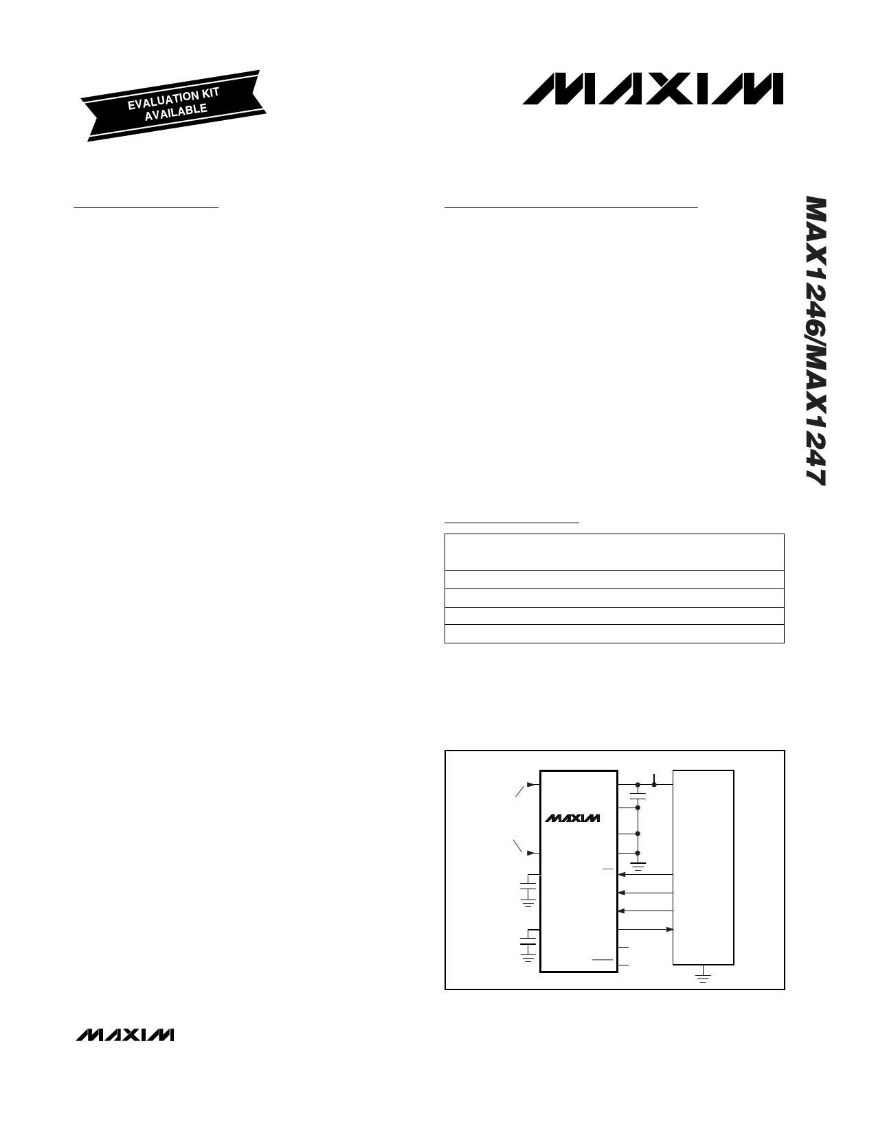
__________Typical Operating Circuit
0V TO
+2.5V
ANALOG
INPUTS
4.7µF
0.047µF
CH0 VDD
DGND
MAX1246 AGND
CH3 COM
VREF
REFADJ
CS
SCLK
DIN
DOUT
SSTRB
SHDN
+3V
VDD
0.1µF
CPU
I/O
SCK (SK)
MOSI (SO)
MISO (SI)
VSS
________________________________________________________________ Maxim Integrated Products 1
For pricing, delivery, and ordering information, please contact Maxim/Dallas Direct! at
1-888-629-4642, or visit Maxim’s website at www.maxim-ic.com.
1 page 
+2.7V, Low-Power, 4-Channel,
Serial 12-Bit ADCs in QSOP-16
ELECTRICAL CHARACTERISTICS (continued)
(VDD = +2.7V to +3.6V (MAX1246); VDD = +2.7V to +5.25V (MAX1247); COM = 0V; fSCLK = 2.0MHz; external clock (50% duty cycle);
15 clocks/conversion cycle (133ksps); MAX1246—4.7µF capacitor at VREF pin; MAX1247—external reference, VREF = 2.5V applied
to VREF pin; TA = TMIN to TMAX; unless otherwise noted.)
PARAMETER
SYMBOL
CONDITIONS
DIGITAL INPUTS (DIN, SCLK, CS, SHDN)
DIN, SCLK, CS Input High Voltage
DIN, SCLK, CS Input Low Voltage
DIN, SCLK, CS Input Hysteresis
DIN, SCLK, CS Input Leakage
DIN, SCLK, CS Input Capacitance
SHDN Input High Voltage
SHDN Input Mid Voltage
SHDN Input Low Voltage
SHDN Input Current
SHDN Voltage, Floating
VIH
VIL
VHYST
IIN
CIN
VSH
VSM
VSL
IS
VFLT
VDD ≤ 3.6V
VDD > 3.6V, MAX1247 only
VIN = 0V or VDD
(Note 7)
SHDN = 0V or VDD
SHDN = FLOAT
SHDN Maximum Allowed
Leakage, Mid Input
SHDN = FLOAT
MIN TYP MAX UNITS
2.0
3.0
0.8
0.2
±0.01 ±1
15
VDD - 0.4
1.1 VDD - 1.1
0.4
±4.0
VDD / 2
±100
V
V
V
µA
pF
V
V
V
µA
V
nA
DIGITAL OUTPUTS (DOUT, SSTRB)
Output Voltage Low
Output Voltage High
Three-State Leakage Current
Three-State Output Capacitance
POWER REQUIREMENTS
VOL
VOH
IL
COUT
Positive Supply Voltage
VDD
Positive Supply Current, MAX1246 IDD
Positive Supply Current, MAX1247 IDD
Supply Rejection (Note 10)
PSR
ISINK = 5mA
ISINK = 16mA
ISOURCE = 0.5mA
CS = VDD
CS = VDD (Note 7)
MAX1246
MAX1247
Operating mode, full-scale input
VDD = 3.6V Fast power-down
Full power-down
Operating mode,
full-scale input
VDD = 5.25V
VDD = 3.6V
Fast power-down
Full power-down
VDD = 5.25V
VDD = 3.6V
VDD = 2.7V to VDD(MAX), full-scale input,
external reference = 2.500V
VDD - 0.5
±0.01
2.70
2.70
1.2
30
1.2
1.8
0.9
30
3.5
1.2
±0.3
0.4
0.8
±10
15
3.60
5.25
2.0
70
10
2.5
1.5
70
15
10
V
V
µA
pF
V
mA
µA
mA
µA
mV
_______________________________________________________________________________________ 5
5 Page 
+2.7V, Low-Power, 4-Channel,
Serial 12-Bit ADCs in QSOP-16
Table 1. Control-Byte Format
BIT 7
(MSB)
BIT 6
BIT 5
START
SEL2
SEL1
BIT 4
SEL0
BIT 3
UNI/BIP
BIT 2
SGL/DIF
BIT 1
PD1
BIT 0
(LSB)
PD0
BIT
7(MSB)
6
5
4
3
NAME
START
SEL2
SEL1
SEL0
UNI/BIP
2 SGL/DIF
1
0(LSB)
PD1
PD0
DESCRIPTION
The first logic “1” bit after CS goes low defines the beginning of the control byte.
These three bits select which of the four channels are used for the conversion (Tables 2 and 3).
1 = unipolar, 0 = bipolar. Selects unipolar or bipolar conversion mode. In unipolar mode, an
analog input signal from 0V to VREF can be converted; in bipolar mode, the signal can range
from -VREF / 2 to +VREF / 2.
1 = single ended, 0 = differential. Selects single-ended or differential conversions. In single-
ended mode, input signal voltages are referred to COM. In differential mode, the voltage
difference between two channels is measured (Tables 2 and 3).
Selects clock and power-down modes.
PD1 PD0 Mode
00
Full power-down
01
Fast power-down
10
Internal clock mode
11
External clock mode
allowed between conversions. The acquisition time,
tACQ, is the maximum time the device takes to acquire
the signal, and is also the minimum time needed for the
signal to be acquired. It is calculated by the following
equation:
tACQ = 9 x (RS + RIN) x 16pF
where RIN = 9kΩ, RS = the source impedance of the
input signal, and tACQ is never less than 1.5µs. Note
that source impedances below 1kΩ do not significantly
affect the ADC’s AC performance.
Higher source impedances can be used if a 0.01µF
capacitor is connected to the individual analog inputs.
Note that the input capacitor forms an RC filter with the
input source impedance, limiting the ADC’s signal
bandwidth.
Input Bandwidth
The ADC’s input tracking circuitry has a 2.25MHz
small-signal bandwidth, so it is possible to digitize
high-speed transient events and measure periodic sig-
nals with bandwidths exceeding the ADC’s sampling
rate by using undersampling techniques. To avoid
high-frequency signals being aliased into the frequency
band of interest, anti-alias filtering is recommended.
Analog Input Protection
Internal protection diodes, which clamp the analog input
to VDD and AGND, allow the channel input pins to swing
from AGND - 0.3V to VDD + 0.3V without damage.
However, for accurate conversions near full scale, the
inputs must not exceed VDD by more than 50mV or be
lower than AGND by 50mV.
If the analog input exceeds 50mV beyond the sup-
plies, do not forward bias the protection diodes of
off channels over 4mA.
How to Start a Conversion
Start a conversion by clocking a control byte into DIN.
With CS low, each rising edge on SCLK clocks a bit from
DIN into the MAX1246/MAX1247’s internal shift register.
After CS falls, the first arriving logic “1” bit defines the
control byte’s MSB. Until this first “start” bit arrives, any
number of logic “0” bits can be clocked into DIN with no
effect. Table 1 shows the control-byte format.
The MAX1246/MAX1247 are compatible with SPI™/
QSPI™ and Microwire™ devices. For SPI, select the
correct clock polarity and sampling edge in the SPI
control registers: set CPOL = 0 and CPHA = 0. Micro-
wire, SPI, and QSPI all transmit a byte and receive a
byte at the same time. Using the Typical Operating
______________________________________________________________________________________ 11
11 Page | ||
| Páginas | Total 25 Páginas | |
| PDF Descargar | [ Datasheet MAX1246.PDF ] | |
Hoja de datos destacado
| Número de pieza | Descripción | Fabricantes |
| MAX1240 | 12-Bit Serial ADCs | Maxim Integrated |
| MAX1241 | 12-Bit Serial ADCs | Maxim Integrated |
| MAX1242 | +2.7V to %.25V / Low-Power / 10-Bit Serial ADCs in SO-8 | Maxim Integrated |
| MAX1243 | +2.7V to %.25V / Low-Power / 10-Bit Serial ADCs in SO-8 | Maxim Integrated |
| Número de pieza | Descripción | Fabricantes |
| SLA6805M | High Voltage 3 phase Motor Driver IC. |
Sanken |
| SDC1742 | 12- and 14-Bit Hybrid Synchro / Resolver-to-Digital Converters. |
Analog Devices |
|
DataSheet.es es una pagina web que funciona como un repositorio de manuales o hoja de datos de muchos de los productos más populares, |
| DataSheet.es | 2020 | Privacy Policy | Contacto | Buscar |