|
|
|
PDF MAX1271 Data sheet ( Hoja de datos )
| Número de pieza | MAX1271 | |
| Descripción | Serial 12-Bit ADCs | |
| Fabricantes | Maxim Integrated | |
| Logotipo | ||
Hay una vista previa y un enlace de descarga de MAX1271 (archivo pdf) en la parte inferior de esta página. Total 20 Páginas | ||
|
No Preview Available !
19-4782; Rev 2; 9/04
EVAALVUAAILTAIOBNLEKIT
Multirange, +5V, 8-Channel,
Serial 12-Bit ADCs
General Description
The MAX1270/MAX1271 are multirange, 12-bit data-
acquisition systems (DAS) that require only a single
+5V supply for operation, yet accept signals at their
analog inputs that can span above the power-supply
rail and below ground. These systems provide eight
analog input channels that are independently software
programmable for a variety of ranges: ±10V, ±5V, 0 to
+10V, 0 to +5V for the MAX1270; ±VREF, ±VREF/2, 0 to
VREF, 0 to VREF/2 for the MAX1271. This range switch-
ing increases the effective dynamic range to 14 bits and
provides the flexibility to interface 4–20mA, ±12V, and
±15V powered sensors directly to a single +5V system.
In addition, these converters are fault protected to
±16.5V; a fault condition on any channel will not affect
the conversion result of the selected channel. Other fea-
tures include a 5MHz bandwidth track/hold, software-
selectable internal/external clock, 110ksps throughput
rate, and internal 4.096V or external reference operation.
The MAX1270/MAX1271 serial interface directly
connects to SPI™/QSPI™ and MICROWIRE™ devices
without external logic.
A hardware shutdown input (SHDN) and two software-
programmable power-down modes, standby (STBYPD)
or full power-down (FULLPD), are provided for low-cur-
rent shutdown between conversions. In standby mode,
the reference buffer remains active, eliminating startup
delays.
The MAX1270/MAX1271 are available in 24-pin narrow
PDIP or space-saving 28-pin SSOP packages.
Applications
Industrial Control Systems
Data-Acquisition Systems
Battery-Powered
Instruments
Automatic Testing
Robotics
Medical Instruments
Ordering Information
PART
TEMP RANGE PIN-PACKAGE
INL
(LSB)
MAX1270ACNG 0°C to +70°C 24 Narrow PDIP
MAX1270BCNG 0°C to +70°C 24 Narrow PDIP
±0.5
±1
MAX1270ACAI 0°C to +70°C 28 SSOP
±0.5
MAX1270BCAI 0°C to +70°C 28 SSOP
±1
Ordering Information continued at end of data sheet.
Features
♦ 12-Bit Resolution, 0.5 LSB Linearity
♦ +5V Single-Supply Operation
♦ SPI/QSPI and MICROWIRE-Compatible
3-Wire Interface
♦ Four Software-Selectable Input Ranges
MAX1270: 0 to +10V, 0 to +5V, ±10V, ±5V
MAX1271: 0 to VREF, 0 to VREF/2, ±VREF,
±VREF/2
♦ Eight Analog Input Channels
♦ 110ksps Sampling Rate
♦ ±16.5V Overvoltage-Tolerant Input Multiplexer
♦ Internal 4.096V or External Reference
♦ Two Power-Down Modes
♦ Internal or External Clock
♦ 24-Pin Narrow PDIP or 28-Pin SSOP Packages
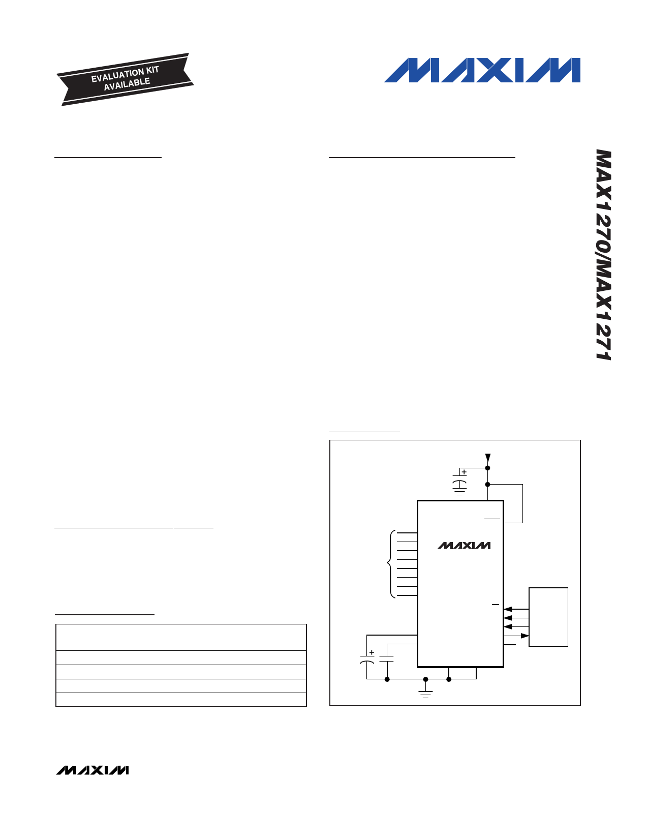
Typical Operating Circuit
+5V
0.1µF
VDD
ANALOG
INPUTS
SHDN
CH0
CH1
CH2
CH3 MAX1270
CH4 MAX1271
CH5
CH6
CH7
REF
REFADJ
CS
SCLK
DIN
DOUT
SSTRB
4.7µF
0.01µF
DGND AGND
MC68HCXX
I/O
SCK
MOSI
MISO
Pin Configurations appear at end of data sheet.
SPI and QSPI are trademarks of Motorola, Inc.
MICROWIRE is a trademark of National Semiconductor Corp.
________________________________________________________________ Maxim Integrated Products 1
For pricing, delivery, and ordering information, please contact Maxim/Dallas Direct! at
1-888-629-4642, or visit Maxim’s website at www.maxim-ic.com.
1 page 
Multirange, +5V, 8-Channel,
Serial 12-Bit ADCs
ELECTRICAL CHARACTERISTICS (continued)
(VDD = +5.0V ±5%; unipolar/bipolar range; external reference mode, VREF = +4.096V; 4.7µF at REF; external clock; fCLK = 2.0MHz,
50% duty cycle (MAX127_B); fCLK = 1.8MHz, 50% duty cycle (MAX127_A); 18 clock/conversion cycle, TA = TMIN to TMAX, unless
otherwise noted. Typical values are TA = +25°C.)
PARAMETER
Conversion Time
Throughput Rate
Bandgap Reference Startup Time
SYMBOL
CONDITIONS
tCONV
External clock mode
(Note 8)
MAX127_A
MAX127_B
Internal clock mode, Figure 9
External clock mode
MAX127_A
MAX127_B
Internal clock mode
Power-up (Note 9)
MIN TYP MAX UNITS
6.6
6.0 µs
6 7.7 11
100
110 ksps
43
200 µs
Reference Buffer Settling Time
To 0.1mV, REF bypass
capacitor fully
discharged
DIGITAL INPUTS (DIN, SCLK, CS, and SHDN)
Input High Threshold Voltage
VIH
Input Low Threshold Voltage
VIL
Input Hysteresis
VHYS
Input Leakage Current
IIN VIN = 0 to VDD
Input Capacitance
CIN (Note 4)
DIGITAL OUTPUTS (DOUT, SSTRB)
Output Voltage Low
VOL ISINK = 5mA
ISINK = 16mA
CREF = 4.7µF
CREF = 33µF
Output Voltage High
VOH
ISOURCE = 0.5mA
Tri-State Leakage Current
Tri-State Output Capacitance
IL
COUT
CS = VDD
CS = VDD (Note 4)
8
ms
60
2.4
0.8
0.2
-10 +10
15
VDD -
0.5
-10
0.4
0.4
+10
15
V
V
V
µA
pF
V
V
µA
pF
_______________________________________________________________________________________ 5
5 Page 
Multirange, +5V, 8-Channel,
Serial 12-Bit ADCs
Table 1. Control-Byte Format
BIT 7
(MSB)
START
BIT 6
SEL2
BIT 5
SEL1
BIT 4
SEL0
BIT 3
RNG
BIT 2
BIP
BIT 1
PD1
BIT
7 (MSB)
6, 5, 4
3
2
1, 0 (LSB)
NAME
START
SEL2, SEL1,
SEL0
RNG
BIP
PD1, PD0
DESCRIPTION
First logic 1 after CS goes low defines the beginning of the control byte.
These 3 bits select the desired “on” channel (Table 2).
Selects the full-scale input voltage range (Table 3).
Selects the unipolar or bipolar conversion mode (Table 3).
Select clock and power-down modes (Table 4).
BIT 0
(LSB)
PD0
Table 2. Channel Selection
SEL2
0
0
0
0
1
1
1
1
SEL1
0
0
1
1
0
0
1
1
SEL0
0
1
0
1
0
1
0
1
CHANNEL
CH0
CH1
CH2
CH3
CH4
CH5
CH6
CH7
Table 4. Power-Down and Clock Selection
PD1 PD0
MODE
0 0 Normal operation (always on), internal clock
mode.
0 1 Normal operation (always on), external clock
mode.
1
0
Standby power-down mode (STBYPD), clock
mode unaffected.
1
1
Full power-down mode (FULLPD), clock mode
unaffected.
Table 3. Range and Polarity Selection for MAX1270/MAX1271
RANGE AND POLARITY SELECTION FOR THE MAX1270
INPUT RANGE
RNG
BIP
Negative
FULL SCALE
0 to +5V
00
—
0 to +10V
10
—
±5V
01
-VREF x 1.2207
±10V
11
-VREF x 2.4414
RANGE AND POLARITY SELECTION FOR THE MAX1271
INPUT RANGE
RNG
BIP
Negative
FULL SCALE
0 to VREF/2
0 to VREF
±VREF/2
±VREF
00
10
01
11
—
—
-VREF/2
-VREF
ZERO
SCALE (V)
0
0
0
0
ZERO
SCALE (V)
0
0
0
0
FULL SCALE
VREF x 1.2207
VREF x 2.4414
VREF x 1.2207
VREF x 2.4414
FULL SCALE
VREF/2
VREF
VREF/2
VREF
______________________________________________________________________________________ 11
11 Page | ||
| Páginas | Total 20 Páginas | |
| PDF Descargar | [ Datasheet MAX1271.PDF ] | |
Hoja de datos destacado
| Número de pieza | Descripción | Fabricantes |
| MAX127 | Multirange / +5V / 12-Bit DAS with 2-Wire Serial Interface | Maxim Integrated |
| MAX1270 | Serial 12-Bit ADCs | Maxim Integrated |
| MAX1271 | Serial 12-Bit ADCs | Maxim Integrated |
| MAX1272 | 12-Bit ADCs | Maxim Integrated |
| Número de pieza | Descripción | Fabricantes |
| SLA6805M | High Voltage 3 phase Motor Driver IC. |
Sanken |
| SDC1742 | 12- and 14-Bit Hybrid Synchro / Resolver-to-Digital Converters. |
Analog Devices |
|
DataSheet.es es una pagina web que funciona como un repositorio de manuales o hoja de datos de muchos de los productos más populares, |
| DataSheet.es | 2020 | Privacy Policy | Contacto | Buscar |