|
|
|
PDF AD7890 Data sheet ( Hoja de datos )
| Número de pieza | AD7890 | |
| Descripción | 12-Bit Serial Data Acquisition System | |
| Fabricantes | Analog Devices | |
| Logotipo | ||
Hay una vista previa y un enlace de descarga de AD7890 (archivo pdf) en la parte inferior de esta página. Total 29 Páginas | ||
|
No Preview Available !
FEATURES
Fast 12-bit ADC with 5.9 μs conversion time
Eight single-ended analog input channels
Selection of input ranges:
±10 V for AD7890-10
0 V to 4.096 V for AD7890-4
0 V to 2.5 V for AD7890-2
Allows separate access to multiplexer and ADC
On-chip track/hold amplifier
On-chip reference
High-speed, flexible, serial interface
Single supply, low-power operation (50 mW maximum)
Power-down mode (75 μW typ)
GENERAL DESCRIPTION
The AD7890 is an 8-channel 12-bit data acquisition system. The
part contains an input multiplexer, an on-chip track/hold
amplifier, a high speed 12-bit ADC, a 2.5 V reference, and a
high speed, serial interface. The part operates from a single 5 V
supply and accepts an analog input range of ±10 V (AD7890-10),
0 V to 4.096 V (AD7890-4), and 0 V to 2.5 V (AD7890-2).
The multiplexer on the part is independently accessible. This
allows the user to insert an antialiasing filter or signal
conditioning, if required, between the multiplexer and the
ADC. This means that one antialiasing filter can be used for all
eight channels. Connection of an external capacitor allows the
user to adjust the time given to the multiplexer settling to
include any external delays in the filter or signal conditioning
circuitry.
Output data from the AD7890 is provided via a high speed
bidirectional serial interface port. The part contains an on-chip
control register, allowing control of channel selection,
conversion start, and power-down via the serial port. Versatile,
high speed logic ensures easy interfacing to serial ports on
microcontrollers and digital signal processors.
In addition to the traditional dc accuracy specifications such as
linearity, full-scale, and offset errors, the AD7890 is also
specified for dynamic performance parameters including
harmonic distortion and signal-to-noise ratio.
LC2MOS 8-Channel, 12-Bit
Serial Data Acquisition System
AD7890
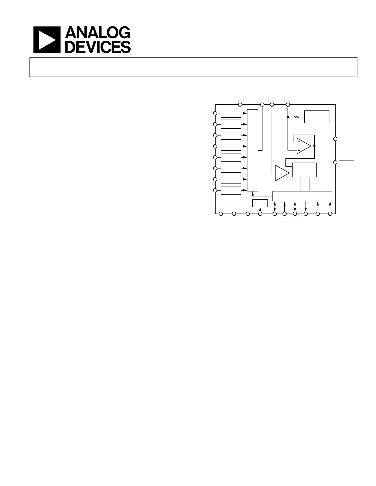
FUNCTIONAL BLOCK DIAGRAM
VDD
MUX SHA REF OUT/
OUT IN REF IN
VIN1
VIN2
VIN3
VIN4
VIN5
VIN6
VIN7
VIN8
SIGNAL
SCALING1
SIGNAL
SCALING1
SIGNAL
SCALING1
SIGNAL
SCALING1
SIGNAL
SCALING1
SIGNAL
SCALING1
SIGNAL
SCALING1
SIGNAL
SCALING1
AD7890
2kΩ 2.5V
REFERENCE
MUX
12-BIT
ADC
TRACK/HOLD
CLOCK
OUTPUT/CONTROL REGISTER
CEXT
CONVST
AGND AGND DGND CLK
IN
SCLK TFS RFS DATA DATA SMODE
OUT IN
1NO SCALING ON AD7890-2
Figure 1.
Power dissipation in normal mode is low at 30 mW typical and the
part can be placed in a standby (power-down) mode if it is not
required to perform conversions. The AD7890 is fabricated in
Analog Devices, Inc.’s Linear Compatible CMOS (LC2MOS)
process, a mixed technology process that combines precision
bipolar circuits with low power CMOS logic. The part is available
in a 24-lead, 0.3" wide, plastic or ceramic dual-in-line package or in
a 24-lead small outline package (SOIC_W).
PRODUCT HIGHLIGHTS
1. Complete 12-Bit Data Acquisition System-on-a-Chip.
The AD7890 is a complete monolithic ADC combining an
8-channel multiplexer, 12-bit ADC, 2.5 V reference, and a
track/hold amplifier on a single chip.
2. Separate Access to Multiplexer and ADC.
The AD7890 provides access to the output of the
multiplexer allowing one antialiasing filter for 8 channels—
a considerable savings over the 8 antialiasing filters required if
the multiplexer is internally connected to the ADC.
3. High Speed Serial Interface.
The part provides a high speed serial interface for easy
connection to serial ports of microcontrollers and DSP
processors.
Rev. C
Information furnished by Analog Devices is believed to be accurate and reliable. However, no
responsibility is assumed by Analog Devices for its use, nor for any infringements of patents or other
rights of third parties that may result from its use. Specifications subject to change without notice. No
license is granted by implication or otherwise under any patent or patent rights of Analog Devices.
Trademarksandregisteredtrademarksarethepropertyoftheirrespectiveowners.
One Technology Way, P.O. Box 9106, Norwood, MA 02062-9106, U.S.A.
Tel: 781.329.4700
www.analog.com
Fax: 781.461.3113
©2006 Analog Devices, Inc. All rights reserved.
1 page 
AD7890
Parameter
LOGIC INPUTS
Input High Voltage, VINH
Input Low Voltage, VINL
Input Current, IIN
Input Capacitance, CIN5
LOGIC OUTPUTS
Output High Voltage, VOH
Output Low Voltage, VOL
Serial Data Output Coding
AD7890-10
AD7890-4
AD7890-2
CONVERSION RATE
Conversion Time
Track/Hold Acquisition Time2, 5
POWER REQUIREMENTS
VDD
IDD (Normal Mode)
IDD (Standby Mode)6 @ 25°C
Power Dissipation
Normal Mode
Standby Mode @ 25°C
A Versions1 B Versions S Version Unit
2.4 2.4 2.4 V min
0.8 0.8 0.8 V max
±10 ±10 ±10 μA max
10 10 10 pF max
4.0 4.0 4.0 V min
0.4 0.4 0.4 V max
Twos Complement
Straight (Natural) Binary
Straight (Natural) Binary
5.9 5.9 5.9 μs max
2 2 2 μs max
5 5 5 V nom
10 10 10 mA max
15 15 15 μA typ
50 50 50 mW max
75 75 75 μW typ
Test Conditions/Comments
VDD = 5 V ± 5%
VDD = 5 V ± 5%
VIN = 0 V to VDD
ISOURCE = 200 μA
ISINK = 1.6 mA
fCLK IN = 2.5 MHz, MUX OUT, connected to
SHA IN
± 5% for specified performance
Logic inputs = 0 V or VDD
Logic inputs = 0 V or VDD
Typically 30 mW
1 Temperature ranges are as follows: A, B Versions: −40°C to +85°C; S Version: −55°C to +125°C.
2 See the Terminology section.
3 This sample rate is only achievable when using the part in external clocking mode.
4 Full-scale error match applies to positive full scale for the AD7890-2 and AD7890-4. It applies to both positive and negative full scale for the AD7890-10.
5 Sample tested @ 25°C to ensure compliance.
6 Analog inputs on AD7890-10 must be at 0 V to achieve correct power-down current.
Rev. C | Page 4 of 28
5 Page 
AD7890
CONTROL REGISTER
The control register for the AD7890 contains 5 bits of information.
Six serial clock pulses must be provided to the part in order to
write data to the control register (seven if the write is required
to put the part in standby mode). If TFS returns high before six
serial clock cycles, then no data transfer takes place to the
control register and the write cycle has to be restarted to write
the data to the control register.
If, however, the CONV bit of the register is set to a Logic 1, then
a conversion is initiated whenever a control register write takes
place regardless of how many serial clock cycles the TFS
remains low for. The default (power-on) condition of all bits in
the control register is 0.
MSB
A2 A1 A0 CONV
LSB
STBY
Table 3.
Bit Name
A2
A1
A0
CONV
STBY
Description
Address Input. This input is the most significant address input for multiplexer channel selection.
Address Input. This is the 2nd most significant address input for multiplexer channel selection.
Address Input. Least significant address input for multiplexer channel selection. When the address is written to the control
register, an internal pulse is initiated, the pulse width of which is determined by the value of capacitance on the CEXT pin. When
this pulse is active, it ensures the conversion process cannot be activated. This allows for the multiplexer settling time,
track/hold acquisition time before the track/hold goes into hold, and the conversion is initiated. In applications where there is
an antialiasing filter between the MUX OUT pin and the SHA IN pin , the filter settling time can be taken into account before the
input on the SHA IN pin is sampled. When the internal pulse times out, the track/hold goes into hold and conversion is initiated.
Conversion Start. Writing a 1 to this bit initiates a conversion in a similar manner to the CONVST input. Continuous conversion
starts do not take place when there is a 1 in this location. The internal pulse and the conversion process are initiated after the
sixth serial clock cycle of the write operation if a 1 is written to this bit. With a 1 in this bit, the hardware conversion start (the
CONVST input) is disabled. Writing a 0 to this bit enables the hardware CONVST input.
Standby Mode Input. Writing a 1 to this bit places the device in its standby, or power-down, mode. Writing a 0 to this bit places
the device in its normal operating mode. The part does not enter its standby mode until the seventh falling edge of SCLK in a
write operation. Therefore, the part requires seven serial clock pulses in its serial write operation if it is required to put the part
into standby.
Rev. C | Page 10 of 28
11 Page | ||
| Páginas | Total 29 Páginas | |
| PDF Descargar | [ Datasheet AD7890.PDF ] | |
Hoja de datos destacado
| Número de pieza | Descripción | Fabricantes |
| AD7890 | 12-Bit Serial Data Acquisition System | Analog Devices |
| AD7891 | 12-Bit High Speed Data Acquisition System | Analog Devices |
| AD7892 | LC2MOS Single Supply/ 12-Bit 600 kSPS ADC | Analog Devices |
| AD7893 | LC2MOS 12-Bit/ Serial 6 us ADC in 8-Pin Package | Analog Devices |
| Número de pieza | Descripción | Fabricantes |
| SLA6805M | High Voltage 3 phase Motor Driver IC. |
Sanken |
| SDC1742 | 12- and 14-Bit Hybrid Synchro / Resolver-to-Digital Converters. |
Analog Devices |
|
DataSheet.es es una pagina web que funciona como un repositorio de manuales o hoja de datos de muchos de los productos más populares, |
| DataSheet.es | 2020 | Privacy Policy | Contacto | Buscar |