|
|
|
PDF AD9944 Data sheet ( Hoja de datos )
| Número de pieza | AD9944 | |
| Descripción | CCD Signal Processors | |
| Fabricantes | Analog Devices | |
| Logotipo | ||
Hay una vista previa y un enlace de descarga de AD9944 (archivo pdf) en la parte inferior de esta página. Total 20 Páginas | ||
|
No Preview Available !
Data Sheet
Complete 10-Bit and 12-Bit, 25 MHz
CCD Signal Processors
AD9943/AD9944
FEATURES
25 MSPS correlated double sampler (CDS)
6 dB to 40 dB 10-bit variable gain amplifier (VGA)
Low noise optical black clamp circuit
Preblanking function
10-bit (AD9943), 12-bit (AD9944) 25 MSPS A/D converter
No missing codes guaranteed
3-wire serial digital interface
3 V single-supply operation
Space-saving 32-lead 5 mm × 5 mm LFCSP package
APPLICATIONS
Digital still cameras
Digital video camcorders
PC cameras
Portable CCD imaging devices
CCTV cameras
GENERAL DESCRIPTION
The AD9943/AD9944 are complete analog signal processors
for CCD applications. They feature a 25 MHz single-channel
architecture designed to sample and condition the outputs of
interlaced and progressive scan area CCD arrays. The signal
chain for the AD9943/AD9944 consists of a correlated double
sampler (CDS), a digitally controlled variable gain amplifier
(VGA), and a black level clamp. The AD9943 offers 10-bit
ADC resolution, while the AD9944 contains a true 12-bit ADC.
The internal registers are programmed through a 3-wire
serial digital interface. Programmable features include gain
adjustment, black level adjustment, input clock polarity, and
power-down modes. The AD9943/AD9944 operate from a
single 3 V power supply, typically dissipate 79 mW, and are
packaged in space-saving 32-lead LFCSP packages.
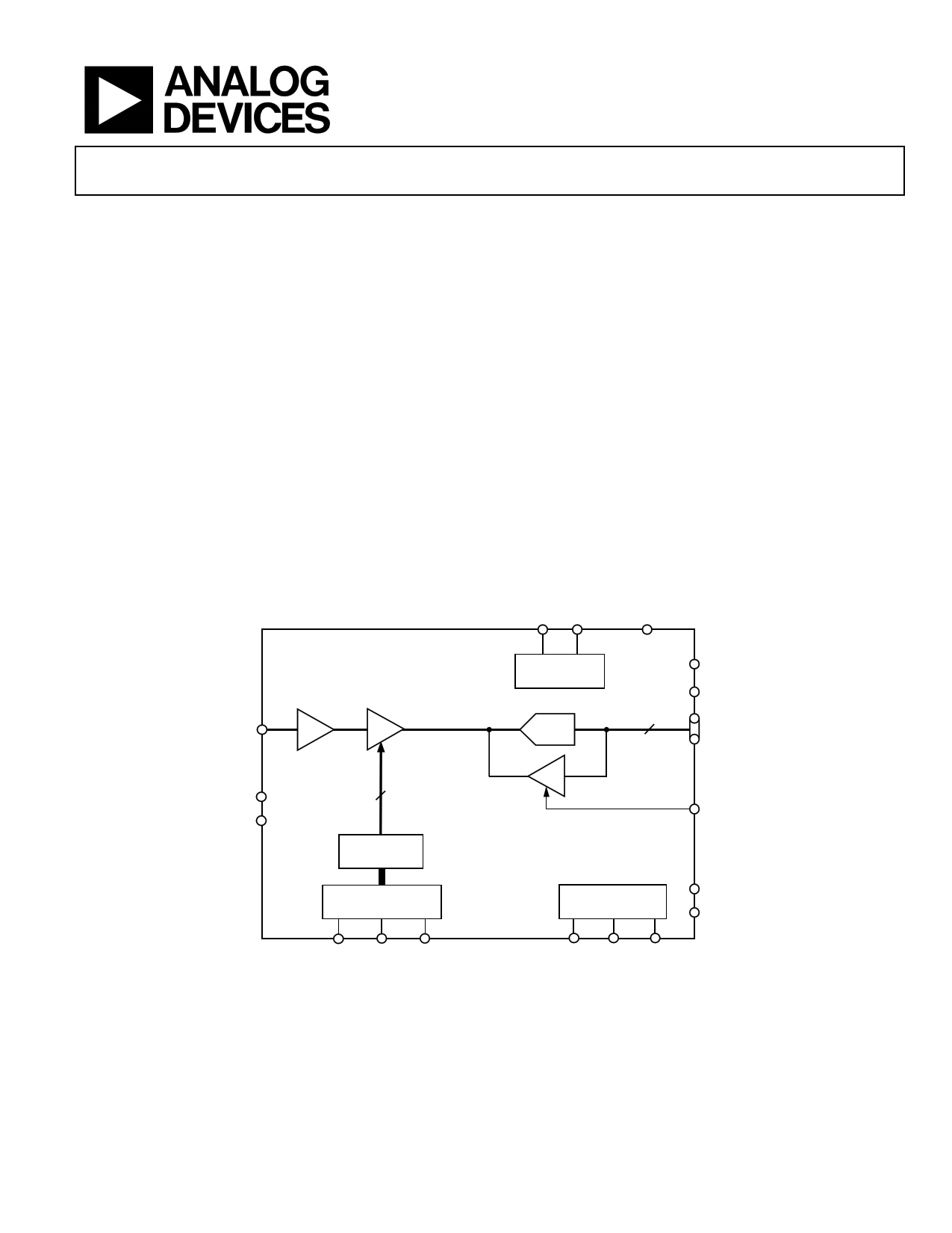
FUNCTIONAL BLOCK DIAGRAM
REFT REFB
PBLK
AD9943/AD9944
CCDIN
CDS
6dB–40dB
VGA
BAND GAP
REFERENCE
10-/12-BIT
ADC
10/12
DRVDD
DRVSS
DOUT
AVDD
AVSS
10
CONTROL
REGISTERS
DIGITAL
INTERFACE
CLP
CLPOB
INTERNAL
TIMING
DVDD
DVSS
SL SCK SDATA
SHP SHD DATACLK
Figure 1. Functional Block Diagram
Rev. C
Document Feedback
Information furnished by Analog Devices is believed to be accurate and reliable. However, no
responsibility is assumed by Analog Devices for its use, nor for any infringements of patents or other
rights of third parties that may result from its use. Specifications subject to change without notice. No
license is granted by implication or otherwise under any patent or patent rights of Analog Devices.
Trademarksandregisteredtrademarksarethepropertyoftheirrespectiveowners.
One Technology Way, P.O. Box 9106, Norwood, MA 02062-9106, U.S.A.
Tel: 781.329.4700 ©2004–2014 Analog Devices, Inc. All rights reserved.
Technical Support
www.analog.com
1 page 
Data Sheet
Parameter
VOLTAGE REFERENCE
Reference Top Voltage (REFT)
Reference Bottom Voltage (REFB)
SYSTEM PERFORMANCE
Gain Range
Low Gain (VGA Code = 0)
Maximum Gain (VGA Code = 1023)
Gain Accuracy
Peak Nonlinearity 500 mV Input Signal
Total Output Noise
Power Supply Rejection (PSR)
1 Input signal characteristics defined as follows:
Min Typ
2.0
1.0
5.3
40 41.5
±1
0.1
0.9
50
500mV TYP
RESET TRANSIENT
100mV TYP
OPTICAL BLACK PIXEL
1V TYP
INPUT SIGNAL RANGE
AD9943/AD9944
Max Unit
Conditions
V
V
Specifications include entire signal chain.
dB
dB
dB
%
LSB rms
dB
12 dB gain applied.
AC grounded input, 6 dB gain applied.
Measured with step change on supply.
TIMING SPECIFICATIONS
CL = 20 pF, fSAMP = 25 MHz. See CCD-mode timing in Figure 14 and Figure 15, and serial timing in Figure 10 and Figure 11.
Table 4.
Parameter
SAMPLE CLOCKS
DATACLK, SHP, SHD Clock Period
DATACLK High/Low Pulse Width
SHP Pulse Width
SHD Pulse Width
CLPOB Pulse Width1
SHP Rising Edge to SHD Falling Edge
SHP Rising Edge to SHD Rising Edge
Internal Clock Delay
DATA OUTPUTS
Output Delay
Pipeline Delay
SERIAL INTERFACE
Maximum SCK Frequency
SL to SCK Setup Time
SCK to SL Hold Time
SDATA Valid to SCK Rising Edge Setup
SCK Falling Edge to SDATA Valid Hold
Symbol
tCONV
tADC
tSHP
tSHD
tCOB
tS1
tS2
tID
tOD
fSCLK
tLS
tLH
tDS
tDH
Min Typ Max Unit
40
16 20
10
10
2 20
10
16 20
3.0
ns
ns
ns
ns
Pixels
ns
ns
ns
9.5 ns
9 Cycles
10 MHz
10 ns
10 ns
10 ns
10 ns
1 Minimum CLPOB pulse width is for functional operation only. Wider typical pulses are recommended to achieve low noise clamp performance.
Rev. C | Page 5 of 20
5 Page 
Data Sheet
TYPICAL PERFORMANCE CHARACTERISTICS
100
90
VDD = 3.3V
80
VDD = 3.0V
70
60 VDD = 2.7V
50
40
10
15 20
SAMPLE RATE (MHz)
25
Figure 7. AD9943/AD9944 Power vs. Sample Rate
0.50
AD9943/AD9944
0.50
0.25
0
–0.25
–0.50
0
800
1600
2400
3200
4000
Figure 9. AD9944 Typical DNL Performance
0.25
0
–0.25
–0.50
0 200 400 600 800 1000
Figure 8. AD9943 Typical DNL Performance
Rev. C | Page 11 of 20
11 Page | ||
| Páginas | Total 20 Páginas | |
| PDF Descargar | [ Datasheet AD9944.PDF ] | |
Hoja de datos destacado
| Número de pieza | Descripción | Fabricantes |
| AD9940 | Correlated Double Sampler | Analog Devices |
| AD9941 | 56 MSPS Imaging Signal Processor | Analog Devices |
| AD9942 | 14-Bit CCD Signal Processor | Analog Devices |
| AD9943 | CCD Signal Processors | Analog Devices |
| Número de pieza | Descripción | Fabricantes |
| SLA6805M | High Voltage 3 phase Motor Driver IC. |
Sanken |
| SDC1742 | 12- and 14-Bit Hybrid Synchro / Resolver-to-Digital Converters. |
Analog Devices |
|
DataSheet.es es una pagina web que funciona como un repositorio de manuales o hoja de datos de muchos de los productos más populares, |
| DataSheet.es | 2020 | Privacy Policy | Contacto | Buscar |