|
|
PDF 8S89831I Data sheet ( Hoja de datos )
| Número de pieza | 8S89831I | |
| Descripción | Differential LVPECL-To-LVPECL/ECL Fanout Buffer | |
| Fabricantes | IDT | |
| Logotipo |  |
|
Hay una vista previa y un enlace de descarga de 8S89831I (archivo pdf) en la parte inferior de esta página. Total 21 Páginas | ||
|
No Preview Available !
Differential LVPECL-To-LVPECL/ECL
Fanout Buffer
8S89831I
Data Sheet
General Description
The 8S89831I is a high speed 1-to-4 Differential- to-LVPECL/ECL
Fanout Buffer. The 8S89831I is optimized for high speed and very
low output skew, making it suitable for use in demanding applications
such as SONET, 1 Gigabit and 10 Gigabit Ethernet, and Fibre
Channel. The internally terminated differential input and VREF_AC pin
allow other differential signal families such as LVDS, LVHSTL and
CML to be easily interfaced to the input with minimal use of external
components. The device also has an output enable pin which may be
useful for system test and debug purposes. The 8S89831I is
packaged in a small 3mm x 3mm 16-pin VFQFN package which
makes it ideal for use in space-constrained applications.
Features
• Four LVPECL/ECL outputs
• IN, nIN input can accept the following differential input levels:
LVPECL, LVDS, CML, SSTL
• 50 internal input termination to VT
• Output frequency: >2.1GHz
• Output skew: 30ps (maximum)
• Part-to-part skew: 185ps (maximum)
• Additive phase jitter, RMS: 0.31ps (typical)
• Propagation Delay: 570ps (maximum)
• LVPECL mode operating voltage supply range:
VCC = 2.5V±5%, 3.3V±5%, VEE = 0V
• ECL mode operating voltage supply range:
VCC = 0V, VEE = -3.3V±5%, -2.5V±5%
• -40°C to 85°C ambient operating temperature
• Available in lead-free (RoHS 6) package
Block Diagram
EN Pullup
DQ
IN
VT 50Ω
nIN 50Ω
VREF_AC
Q0
nQ0
Q1
nQ1
Q2
nQ2
Q3
nQ3
Pin Assignment
16 15 14 13
Q1 1
12 IN
nQ1 2
11 VT
Q2 3
10 VREF_AC
nQ2 4
9 nIN
5 6 78
8S89831I
16-Lead VFQFN
3mm x 3mm x 0.925mm package body
K Package
Top View
©2016 Integrated Device Technology, Inc
1
Revision A January 27, 2016
1 page 
8S89831I Data Sheet
Table 4C. Differential DC Characteristics, VCC = 2.5V ± 5%, 3.3V ± 5%, TA = -40°C to 85°C
Symbol Parameter
Test Conditions
Minimum
Typical
RIN
VIH
VIL
VIN
VDIFF_IN
IIN
VREF_AC
Differential Input Resistance (IN, nIN)
Input High Voltage
(IN, nIN)
Input Low Voltage
(IN, nIN)
Input Voltage Swing
Differential Input Voltage Swing
Input Current; NOTE 1
(IN, nIN)
Bias Voltage
IN to VT, nIN to VT
40 50
1.2
0
0.15
0.3
VCC – 1.45 VCC – 1.37
NOTE 1: Guaranteed by design.
Maximum
60
VCC
VIH – 0.15
1.2
35
VCC – 1.32
Units
V
V
V
V
mA
V
Table 4D. LVPECL DC Characteristics, VCC = 2.5V ± 5%, 3.3V ± 5%, TA = -40°C to 85°C
Symbol Parameter
Test Conditions
Minimum
VOH Output High Voltage; NOTE 1
VOL Output Low Voltage; NOTE 1
VOUT
Output Voltage Swing
VDIFF_OUT Differential Output Voltage Swing
VCC – 1.175
VCC – 2.0
0.6
1.2
NOTE 1: Outputs terminated with 50 to VCC – 2V.
Typical
Maximum
VCC – 0.85
VCC – 1.575
1.0
2.0
Units
V
V
V
V
©2016 Integrated Device Technology, Inc
5
Revision A January 27, 2016
5 Page 
8S89831I Data Sheet
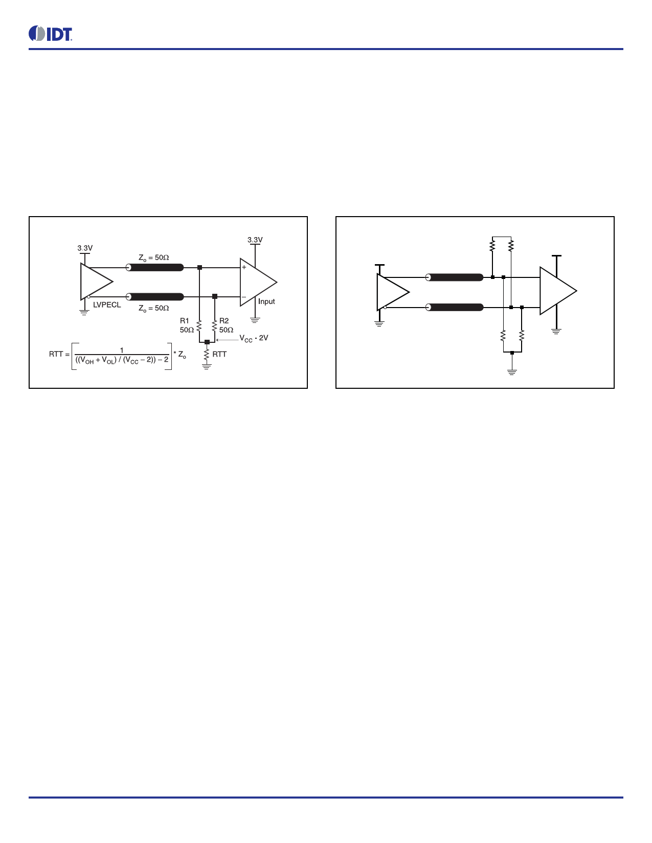
Termination for 3.3V LVPECL Outputs
The clock layout topology shown below is a typical termination for
LVPECL outputs. The two different layouts mentioned are
recommended only as guidelines.
The differential outputs are low impedance follower outputs that
generate ECL/LVPECL compatible outputs. Therefore, terminating
resistors (DC current path to ground) or current sources must be
used for functionality. These outputs are designed to drive 50
transmission lines. Matched impedance techniques should be used
to maximize operating frequency and minimize signal distortion.
Figures 4A and 4B show two different layouts which are
recommended only as guidelines. Other suitable clock layouts may
exist and it would be recommended that the board designers
simulate to guarantee compatibility across all printed circuit and clock
component process variations.
3.3V
3.3V
R3 R4
125
125
3.3V
Zo = 50
+
Zo = 50
R1
84
_
R2
84
Input
Figure 4A. 3.3V LVPECL Output Termination
Figure 4B. 3.3V LVPECL Output Termination
©2016 Integrated Device Technology, Inc
11
Revision A January 27, 2016
11 Page | ||
| Páginas | Total 21 Páginas | |
| PDF Descargar | [ Datasheet 8S89831I.PDF ] | |
Hoja de datos destacado
| Número de pieza | Descripción | Fabricantes |
| 8S89831I | Differential LVPECL-To-LVPECL/ECL Fanout Buffer | IDT |
| Número de pieza | Descripción | Fabricantes |
| SLA6805M | High Voltage 3 phase Motor Driver IC. |
Sanken |
| SDC1742 | 12- and 14-Bit Hybrid Synchro / Resolver-to-Digital Converters. |
Analog Devices |
|
DataSheet.es es una pagina web que funciona como un repositorio de manuales o hoja de datos de muchos de los productos más populares, |
| DataSheet.es | 2020 | Privacy Policy | Contacto | Buscar |
