|
|
|
PDF 8T74S208 Data sheet ( Hoja de datos )
| Número de pieza | 8T74S208 | |
| Descripción | 2.5V Differential LVDS Clock Divider and Fanout Buffer | |
| Fabricantes | IDT | |
| Logotipo | ||
Hay una vista previa y un enlace de descarga de 8T74S208 (archivo pdf) en la parte inferior de esta página. Total 18 Páginas | ||
|
No Preview Available !
2.5V Differential LVDS Clock Divider
and Fanout Buffer
8T74S208
DATA SHEET
General Description
The 8T74S208 is a high-performance differential LVDS clock divider
and fanout buffer. The device is designed for the frequency division
and signal fanout of high-frequency, low phase-noise clocks. The
8T74S208 is characterized to operate from a 2.5V power supply.
Guaranteed output-to-output and part-to-part skew characteristics
make the 8T74S208 ideal for those clock distribution applications
demanding well-defined performance and repeatability. The
integrated input termination resistors make interfacing to the
reference source easy and reduce passive component count. Each
output can be individually enabled or disabled in the high-impedance
state controlled by a I2C register. On power-up, all outputs are
enabled.
Features
• One differential input reference clock
• Differential pair can accept the following differential input
levels: LVDS, LVPECL, CML
• Integrated input termination resistors
• Eight LVDS outputs
• Selectable clock frequency division of ÷1, ÷2, ÷4 and ÷8
• Maximum input clock frequency: 1GHz
• LVCMOS interface levels for the control inputs
• Individual output enabled/ disabled by I2C interface
• Output skew: 45ps (maximum)
• Output rise/fall times: 350ps (maximum)
• Low additive phase jitter, RMS: 96fs (typical)
• Full 2.5V supply voltage
• Outputs enabled at power up
• Lead-free (RoHS 6) 32-Lead VFQFN packaging
• -40°C to 85°C ambient operating temperature
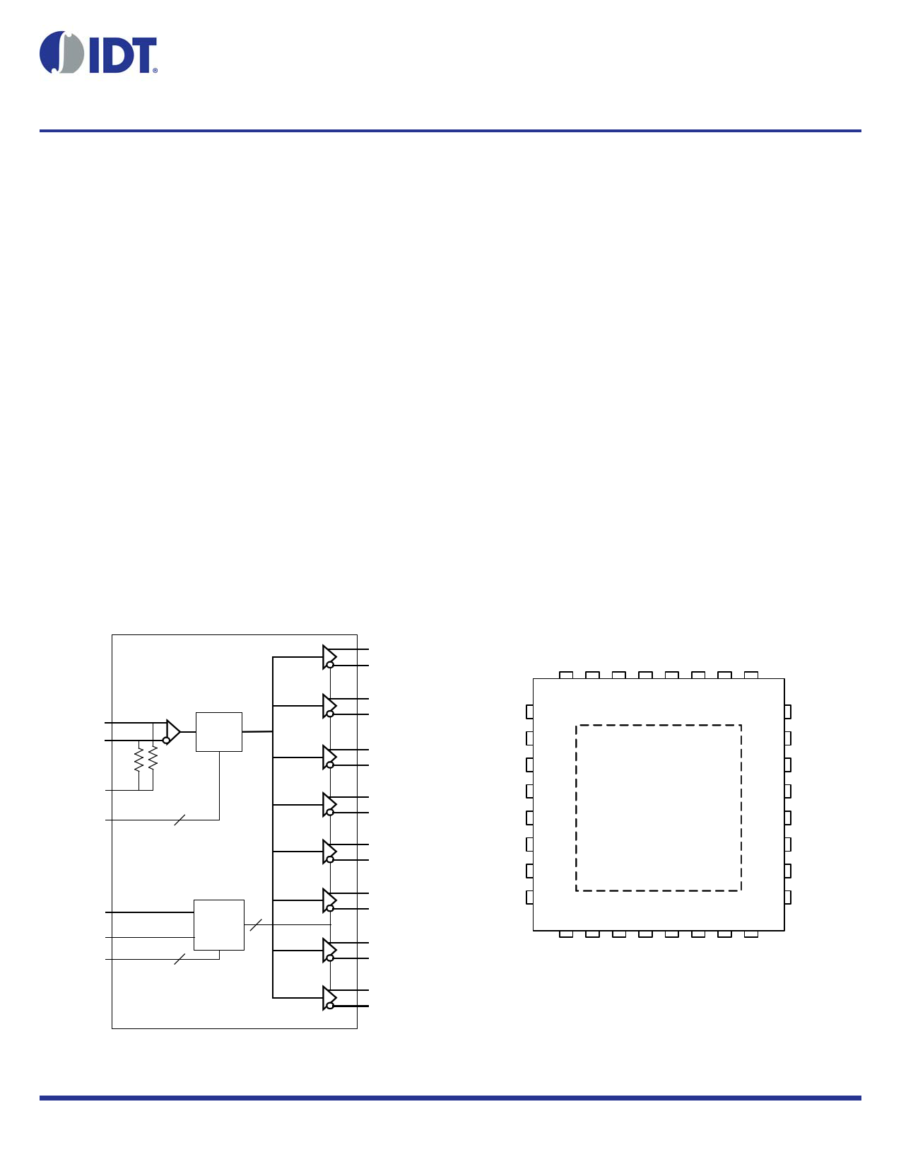
Block Diagram
IN
nIN
50
fREF
÷1, ÷2,
÷4, ÷8
50
VT
FSEL[1:0] Pulldown (2)
2
SDA Pullup
SCL Pullup
ADR[1:0] Pulldown (2)
2
I2C
8
Pin Assignment
Q0
nQ0
Q1
nQ1
Q2
nQ2
Q3
nQ3
Q4
nQ4
Q5
nQ5
Q6
nQ6
ADR1
GND
Q0
nQ0
Q1
nQ1
GND
VDDO
32 31 30 29 28 27 26 25
1 24
2 23
3 22
4 21
8T74S208
5 20
6 19
7 18
8 17
9 10 11 12 13 14 15 16
FSEL0
GND
nQ7
Q7
nQ6
Q6
GND
VDDO
Q7 32-Lead VFQFN
nQ7 5mm x 5mm x 0.925mm
package body
NL Package, Top View
8T74S208 REVISION 1 09/10/14
1 ©2014 Integrated Device Technology, Inc.
1 page 
8T74S208 DATA SHEET
Table 4C. Differential Input DC Characteristics, VDD = VDDO = 2.5V ± 5%, TA = -40°C to 85°C
Symbol Parameter
Test Conditions
Minimum Typical Maximum Units
VIN
VCMR
VDIFF
Input Voltage Swing
IN, nIN
Common Mode Input Voltage1 2
Differential Input Voltage IN, nIN
Swing
0.15
1.2
0.3
1.2
VDD – (VPP/2)
2.4
V
V
V
RIN Input Resistance
IN, nIN to VT
Differential
RIN, DIFF Input Resistance
IN to nIN,
VT = open
NOTE: 1. Common Mode Input Voltage is defined as the crosspoint.
NOTE: 2. VIL should not be less than -0.3V and VIH should not be greater than VDD.
40 50
60
80 100 120
.
Table 4D. LVDS DC Characteristics, VDD = VDDO = 2.5V, TA = -40°C to 85°C
Symbol Parameter
Test Conditions
VOD
VOD
VOS
VOS
Differential Output Voltage
VOD Magnitude Change
Offset Voltage
VOS Magnitude Change
Minimum
247
1.120
Typical
Maximum
454
50
1.425
50
Units
mV
mV
V
mV
REVISION 1 09/10/14
5 2.5V DIFFERENTIAL LVDS CLOCK DIVIDER AND FANOUT BUFFER
5 Page 
8T74S208 DATA SHEET
VFQFN EPAD Thermal Release Path
In order to maximize both the removal of heat from the package and
the electrical performance, a land pattern must be incorporated on
the Printed Circuit Board (PCB) within the footprint of the package
corresponding to the exposed metal pad or exposed heat slug on the
package, as shown in Figure 5. The solderable area on the PCB, as
defined by the solder mask, should be at least the same size/shape
as the exposed pad/slug area on the package to maximize the
thermal/electrical performance. Sufficient clearance should be
designed on the PCB between the outer edges of the land pattern
and the inner edges of pad pattern for the leads to avoid any shorts.
While the land pattern on the PCB provides a means of heat transfer
and electrical grounding from the package to the board through a
solder joint, thermal vias are necessary to effectively conduct from
the surface of the PCB to the ground plane(s). The land pattern must
be connected to ground through these vias. The vias act as “heat
pipes”. The number of vias (i.e. “heat pipes”) are application specific
and dependent upon the package power dissipation as well as
electrical conductivity requirements. Thus, thermal and electrical
analysis and/or testing are recommended to determine the minimum
number needed. Maximum thermal and electrical performance is
achieved when an array of vias is incorporated in the land pattern. It
is recommended to use as many vias connected to ground as
possible. It is also recommended that the via diameter should be 12
to 13mils (0.30 to 0.33mm) with 1oz copper via barrel plating. This is
desirable to avoid any solder wicking inside the via during the
soldering process which may result in voids in solder between the
exposed pad/slug and the thermal land. Precautions should be taken
to eliminate any solder voids between the exposed heat slug and the
land pattern. Note: These recommendations are to be used as a
guideline only. For further information, please refer to the Application
Note on the Surface Mount Assembly of Amkor’s Thermally/
Electrically Enhance Lead frame Base Package, Amkor Technology.
PIN SOLDER
EXPOSED HEAT SLUG
SOLDER
PIN
PIN PAD
GROUND PLANE
THERMAL VIA
LAND PATTERN
(GROUND PAD)
PIN PAD
Figure 5. P.C. Assembly for Exposed Pad Thermal Release Path – Side View (drawing not to scale)
Recommendations for Unused Input and Output Pins
Inputs:
Outputs:
LVCMOS Control Pins
All control pins have internal pullup or pulldown resistors; additional
resistance is not required but can be added for additional protection.
A 1k resistor can be used.
LVDS Outputs
All unused LVDS output pairs can be either left floating or terminated
with 100 across. If they are left floating, there should be no trace
attached.
REVISION 1 09/10/14
11 2.5V DIFFERENTIAL LVDS CLOCK DIVIDER AND FANOUT BUFFER
11 Page | ||
| Páginas | Total 18 Páginas | |
| PDF Descargar | [ Datasheet 8T74S208.PDF ] | |
Hoja de datos destacado
| Número de pieza | Descripción | Fabricantes |
| 8T74S208 | 2.5V Differential LVDS Clock Divider and Fanout Buffer | IDT |
| 8T74S208A-01 | 2.5V Differential LVDS Clock Divider and Fanout Buffer | IDT |
| 8T74S208C-01 | 2.5 V Differential LVDS Clock Divider and Fanout Buffer | IDT |
| Número de pieza | Descripción | Fabricantes |
| SLA6805M | High Voltage 3 phase Motor Driver IC. |
Sanken |
| SDC1742 | 12- and 14-Bit Hybrid Synchro / Resolver-to-Digital Converters. |
Analog Devices |
|
DataSheet.es es una pagina web que funciona como un repositorio de manuales o hoja de datos de muchos de los productos más populares, |
| DataSheet.es | 2020 | Privacy Policy | Contacto | Buscar |