|
|
|
PDF 9FGP202A Data sheet ( Hoja de datos )
| Número de pieza | 9FGP202A | |
| Descripción | FREQUENCY TIMING GENERATOR | |
| Fabricantes | IDT | |
| Logotipo | ||
Hay una vista previa y un enlace de descarga de 9FGP202A (archivo pdf) en la parte inferior de esta página. Total 19 Páginas | ||
|
No Preview Available !
FREQUENCY TIMING GENERATOR FOR PERIPHERALS
DATASHEET
9FGP202A
General Description
The 9FGP202A is a peripheral clock for Intel Server. It is
driven with a 25MHz crystal and generates CPU outputs up
to 400MHz. An SMBus interface allows full control of the
device.
Recommended Application
Peripheral Clock for Intel Server
Output Features
• 1 - 0.7V current-mode differential CPU pair
• 8 - 50MHz output
• 1 - DOT 96MHz output
• 1 - 33.33MHz output
• 1 - 32.768KHz output
• 2 - 25MHz REF outputs
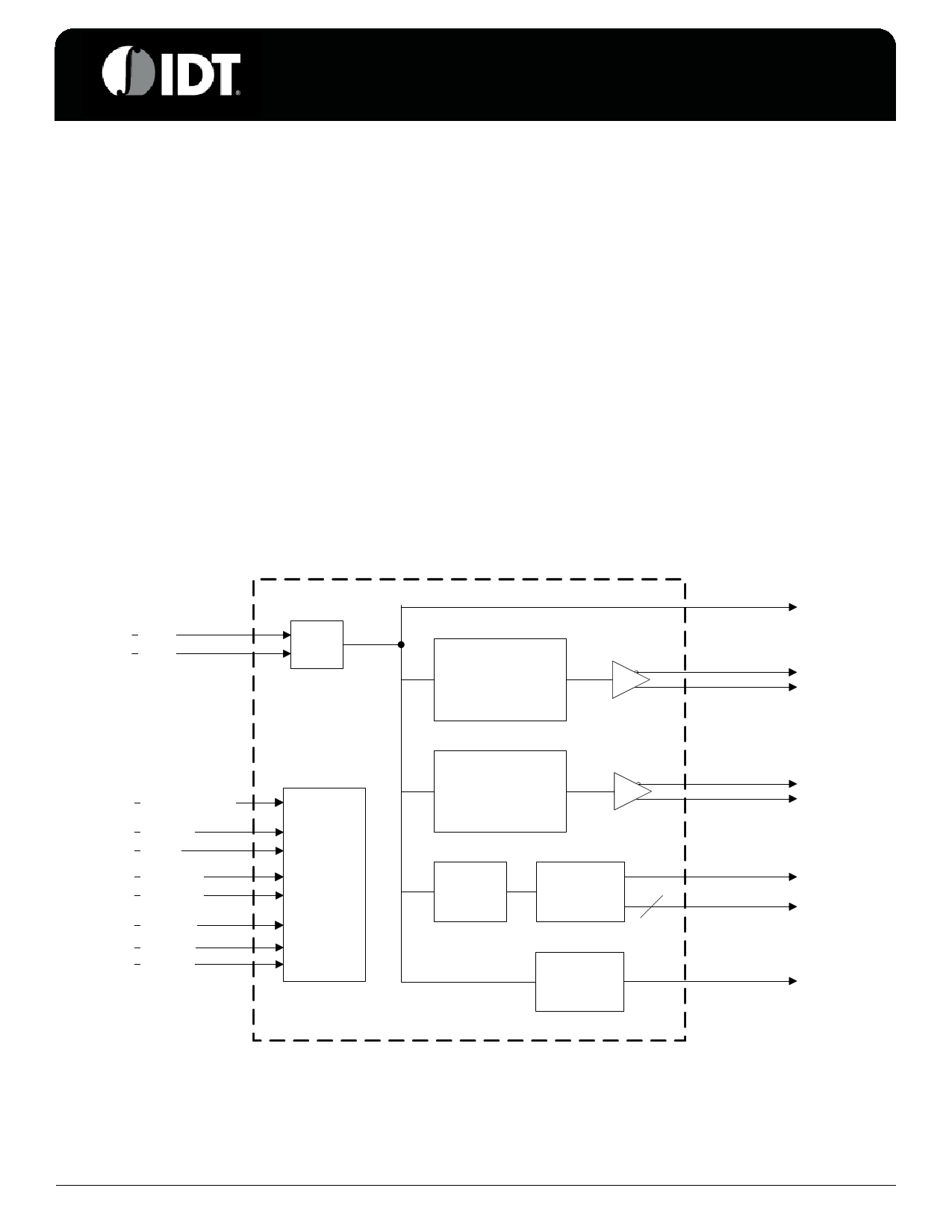
Block Diagram
Features/Benefits
• Selectable SMBus Address – D0/D1 or C0/C1
• Spread Spectrum capability on CPU and DOT 96MHz
clocks
• SMBus Control:
– M/N and spread programming on CPU and DOT
96MHz clocks via SMBus
– Outputs can be disabled via pins or SMBus
Key Specifications
• Exact synthesis on CPU, RMII and 33.33MHz clocks
• +/- 100ppm frequency accuracy on remaining clocks
X1_25
X2_25
XTAL
CPU PLL
(SPREAD
CAPABLE)
25MHz(1:0)
CPUCLK
VttPwr_GD/PD#
OE_CPU
OE_96
OE_RMIIA
OE_RMIIB
SMBADR
SMBDAT
SMBCLK
CONTROL
LOGIC
DOT PLL
(SPREAD
CAPABLE)
FIXED
PLL
DIVIDERS
8
DIVIDERS
DOT96SS
33.33MHz
RMII(7:0)
32.768KHz
IDT® FREQUENCY TIMING GENERATOR FOR PERIPHERALS
1
9FGP202A
REV D 070511
1 page 
9FGP202A
FREQUENCY TIMING GENERATOR FOR PERIPHERALS
Truth Table 1: VttPwr_GD/PD# and OE_96
V ttPwr_ GD/ PD#
Pin 40
0
0
1
1
OE_96
Pin 5
0
1
0
1
Clocks
All clocks are powered down
All clocks are powered down
All clocks are enabled except DOT96SS
*All clocks are enabled including DOT96SS
*Assuming DOT96 Output Enable from SMBus Byte2 Bit0 sets to enable (default)
Truth Table 2: VttPwr_GD/PD# and OE_CPU
V ttPwr_ GD/ PD#
Pin 40
0
0
1
1
OE_ CPU
Pin 6
0
1
0
1
Clocks
All clocks are powered down
All clocks are powered down
All clocks are enabled except CPUCLK
*All clocks are enabled including CPUCLK
*Assuming CPUCLK Output Enable from SMBus Byte2 Bit1 sets to enable (default)
Table 1: CPU Spread and Frequency Selection
CPU
CPU
CPU
CPU
SS_EN
F S2
FS1
FS0 CPU
Byte 0
Byte 0
Byte 0
Byte 0
MH z
Bit 3
0
0
Bit 2
0
0
Bit 1
0
0
Bit 0
0
1
266.67
133.33
0 0 1 0 200.00
0 0 1 1 166.67
0 1 0 0 333.33
0 1 0 1 100.00
0 1 1 0 400.00
0 1 1 1 200.00
1 0 0 0 266.67
1 0 0 1 133.33
1 0 1 0 200.00
1 0 1 1 166.67
1 1 0 0 333.33
1 1 0 1 100.00
1 1 1 0 400.00
1 1 1 1 200.00
Do wn
Spread %
0%
0%
0%
0%
0%
0%
0%
0%
0.5%
0.5%
0.5%
0.5%
0.5%
0.5%
0.5%
0.5%
IDT® FREQUENCY TIMING GENERATOR FOR PERIPHERALS
5
9FGP202A
REV D 070511
5 Page 
9FGP202A
FREQUENCY TIMING GENERATOR FOR PERIPHERALS
Electrical Characteristics–32.768kHz
P ARAMETE R
SYMB OL
CONDITIONS*
MIN
TYP
MAX UNITS NOTES
Long Accuracy
ppm
see Tperiod min-max values
-1 00
100 ppm 1
Clock period
Tperiod
32.768KHz output nominal
30.518
us 1
Output High Voltage
VOH
IOH = -1 mA
2.4
V1
Output Low Voltage
VOL
IOL = 1 mA
0.4 V 1
Output High Current
IOH V OH @ MIN = 1.0 V -33
VOH@MAX = 3.135 V
mA 1
-33 mA 1
Output Low Current
Rise Time
Fall Time
IOL
VOL @ MIN = 1.95 V
V OL @ MAX = 0.4 V
30
tr VOL = 0.4 V , VOH = 2.4 V 1
tf VOH = 2.4 V , VOL = 0.4 V 1
mA 1
38 mA 1
4 ns 1
4 ns 1
Duty Cycle dt1 VT = 1.5 V 45
55 % 1
Jitter, Cycle to cycle
tjcyc -cyc
VT = 1.5 V
500 ps 1
*TA = 0 - 70°C; S upply Voltage VDD = 3.3 V +/-5%, CL = 5 pF with Rs as shown i n the termination table (unless otherwise specified)
1Guaranteed by desig n and characterization, not 100% tested in production.
Electrical Characteristics–REF - 25MHz
P ARAMETE R
SYMB OL
CONDITIONS
MIN TYP MAX UNITS
Long Accuracy
ppm see Tperiod min-max values
-50
50 ppm
Clock period
Outp ut High Volta ge
Output Low Voltage
Output High Current
Output Low Current
Rise Time
Fall Time
Tpe rio d
VOH
V OL
IOH
IOL
tr1
tf1
25.00MHz output nominal
IOH = -1 mA
IOL = 1 mA
V OH @MIN = 1.0 V
VOH@MAX = 3.135 V
VOL @ MIN = 1.95 V
V OL @ MAX = 0.4 V
VOL = 0.4 V, VOH = 2.4 V
VOH = 2.4 V, VOL = 0.4 V
39.980
2.4
-29
29
1
1
40.000
40.020
0.4
-23
27
2
2
ns
V
V
mA
mA
mA
mA
ns
ns
Skew
tsk1 VT = 1.5 V
500 ps
Duty Cycle dt1 VT = 1.5 V 45
55 %
Ji tter
tjcyc -cyc
VT = 1.5 V
500 ps
*TA = 0 - 70°C; S upply Voltage VDD = 3.3 V +/-5%, CL = 5 pF with Rs as shown i n the termination table (unless otherwise specified)
1Guaranteed by desig n and characterization, not 100% tested in production.
2 All Long Term Accuracy and Clock Period specifications are guaranteed assuming that REFOUT is at 25.000MHz
Notes
1,2
2
1
1
1
1
1
1
1
1
1
1
1
IDT® FREQUENCY TIMING GENERATOR FOR PERIPHERALS
11
9FGP202A
REV D 070511
11 Page | ||
| Páginas | Total 19 Páginas | |
| PDF Descargar | [ Datasheet 9FGP202A.PDF ] | |
Hoja de datos destacado
| Número de pieza | Descripción | Fabricantes |
| 9FGP202A | FREQUENCY TIMING GENERATOR | IDT |
| Número de pieza | Descripción | Fabricantes |
| SLA6805M | High Voltage 3 phase Motor Driver IC. |
Sanken |
| SDC1742 | 12- and 14-Bit Hybrid Synchro / Resolver-to-Digital Converters. |
Analog Devices |
|
DataSheet.es es una pagina web que funciona como un repositorio de manuales o hoja de datos de muchos de los productos más populares, |
| DataSheet.es | 2020 | Privacy Policy | Contacto | Buscar |