|
|
|
PDF 853S111B Data sheet ( Hoja de datos )
| Número de pieza | 853S111B | |
| Descripción | LVPECL/ECL Fanout Buffer | |
| Fabricantes | IDT | |
| Logotipo | ||
Hay una vista previa y un enlace de descarga de 853S111B (archivo pdf) en la parte inferior de esta página. Total 25 Páginas | ||
|
No Preview Available !
Low Skew, 1-to-10, Differential-to-2.5V,
3.3V LVPECL/ECL Fanout Buffer
853S111B
DATA SHEET
General Description
The 853S111B is a low skew, high performance 1-to-10
Differential-to-2.5V/ 3.3V LVPECL/ECL Fanout Buffer. The
853S111B is characterized to operate from either a 2.5V or a 3.3V
power supply. Guaranteed output and part-to-part skew
characteristics make the 853S111B ideal for those clock distribution
applications demanding well defined performance and repeatability.
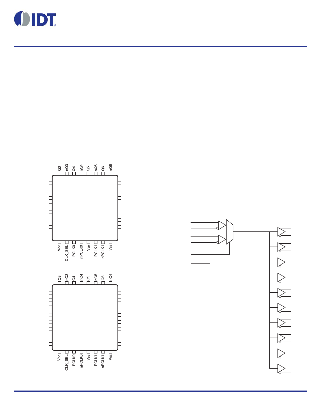
Pin Assignments
VCCO
nQ2
Q2
nQ1
Q1
nQ0
Q0
VCCO
24 23 22 21 20 19 18 17
25 16
26 853S111B 15
27 32-Lead TQFP, E-Pad 14
28 7mm x 7mm x 1mm 13
29 package body 12
30 Y Package 11
31 Top View 10
32 9
12 3 45 6 78
VCCO
Q7
nQ7
Q8
nQ8
Q9
nQ9
VCCO
VCCO
nQ2
Q2
nQ1
Q1
nQ0
Q0
VCCO
24 23 22 21 20 19 18 17
25 16
26 853S111B 15
27 32-Lead VFQFN 14
28 5mm x 5mm x 0.925mm 13
29 package body 12
30 K Package 11
31 Top View 10
32 9
12 3 45 6 78
VCCO
Q7
nQ7
Q8
nQ8
Q9
nQ9
VCCO
Features
• Ten differential 2.5V, 3.3V LVPECL/ECL outputs
• Two selectable differential input pairs
• PCLKx, nPCLKx pairs can accept the following
differential input levels: LVPECL, LVDS, SSTL, CML
• Maximum output frequency: 2.5GHz
• Translates any single-ended input signal to 3.3V LVPECL levels
with resistor bias on nPCLK input
• Output skew: 50ps (maximum)
• Part-to-part skew: 150ps (maximum)
• Propagation delay: 645ps (maximum)
• Additive Phase Jitter, RMS: 0.03ps (typical)
• LVPECL mode operating voltage supply range:
VCC = 2.375V to 3.8V, VEE = 0V
• ECL mode operating voltage supply range:
VCC = 0V, VEE = -3.8V to -2.375V
• -40°C to 85°C ambient operating temperature
• Available lead-free (RoHS 6) packaging
Block Diagram
PCLK0 Pulldown
nPCLK0 Pullup/Pulldown
PCLK1 Pulldown
nPCLK1 Pullup/Pulldown
CLK_SEL Pulldown
VBB
0
1
Q0
nQ0
Q1
nQ1
Q2
nQ2
nQ3
nQ3
Q4
nQ4
Q5
nQ5
Q6
nQ6
Q7
nQ7
nQ8
nQ8
Q9
nQ9
853S111B REVISION E 6/30/15
1 ©2015 Integrated Device Technology, Inc.
1 page 
853S111B DATA SHEET
Table 4B. LVPECL DC Characteristics, VCC = VCCO = 3.3V; VEE = 0V, TA = -40°C to 85°C
-40°C
25°C
Symbol Parameter
Min Typ Max Min Typ Max
VOH Output High Voltage; NOTE 1
2.175 2.275 2.445 2.225 2.295 2.445
VOL Output Low Voltage; NOTE 1
1.405 1.545 1.70 1.375 1.52 1.645
VIH Input High Voltage (Single-ended) 2.075
2.36 2.075
2.36
VIL
Input Low Voltage (Single-ended)
1.43
1.765 1.43
1.765
VBB
Output Voltage Reference;
NOTE 2
1.86
1.98 1.86
1.98
VPP
Peak-to-Peak Input Voltage;
NOTE 3
150 800 1300 150 800 1200
VCMR1
Input High Voltage Common Mode
Range; NOTE 3, 4
1.3
3.3 1.2
3.3
VCMR2
Input Voltage Common Mode Range
referenced to Cross-point; NOTE 3,
5
1.3 -
VPP/2
3.3 - 1.2 -
VPP/2 VPP/2
3.3 -
VPP/2
IIH
Input
PCLK0, PCLK1
High Current nPCLK0, nPCLK1
200 200
IIL
Input
PCLK0, PCLK1
Low Current nPCLK0, nPCLK1
-10
-200
-10
-200
Min
2.215
1.355
2.075
1.43
1.86
150
1.2
1.2 -
VPP/2
-10
-200
85°C
Typ
2.33
1.535
800
Max
2.410
1.63
2.36
1.765
1.98
1200
3.3
3.3 -
VPP/2
200
Units
V
V
V
V
V
mV
V
V
µA
µA
µA
NOTE: Input and output parameters vary 1:1 with VCC. VEE can vary +0.925V to -0.5V.
NOTE 1: Outputs terminated with 50 to VCCO – 2V.
NOTE 2: Single-ended input operation is limited. VCC 3V in LVPECL mode.
NOTE 3: VIL should not be less than VEE – 0.3V, VIH should not be greater than VCC.
NOTE 4: Common mode voltage is defined as VIH.
NOTE 5: Common mode voltage is defined as VCROSS-POINT.
REVISION E 6/30/15
5 LOW SKEW, 1-TO-10, DIFFERENTIAL-TO-2.5V, 3.3V LVPECL/ECL
FANOUT BUFFER
5 Page 
Applications Information
853S111B DATA SHEET
Wiring the Differential Input to Accept Single-Ended Levels
Figure 1 shows how a differential input can be wired to accept single
ended levels. The reference voltage V1= VCC/2 is generated by the
bias resistors R1 and R2. The bypass capacitor (C1) is used to help
filter noise on the DC bias. This bias circuit should be located as close
to the input pin as possible. The ratio of R1 and R2 might need to be
adjusted to position the V1in the center of the input voltage swing. For
example, if the input clock swing is 2.5V and VCC = 3.3V, R1 and R2
value should be adjusted to set V1 at 1.25V. The values below are for
when both the single ended swing and VCC are at the same voltage.
This configuration requires that the sum of the output impedance of
the driver (Ro) and the series resistance (Rs) equals the transmission
line impedance. In addition, matched termination at the input will
attenuate the signal in half. This can be done in one of two ways.
First, R3 and R4 in parallel should equal the transmission line
impedance. For most 50 applications, R3 and R4 can be 100. The
values of the resistors can be increased to reduce the loading for
slower and weaker LVCMOS driver. When using single-ended
signaling, the noise rejection benefits of differential signaling are
reduced. Even though the differential input can handle full rail
LVCMOS signaling, it is recommended that the amplitude be
reduced. The datasheet specifies a lower differential amplitude,
however this only applies to differential signals. For single-ended
applications, the swing can be larger, however VIL cannot be less
than -0.3V and VIH cannot be more than VCC + 0.3V. Though some
of the recommended components might not be used, the pads
should be placed in the layout. They can be utilized for debugging
purposes. The datasheet specifications are characterized and
guaranteed by using a differential signal.
Figure 1. Recommended Schematic for Wiring a Differential Input to Accept Single-ended Levels
REVISION E 6/30/15
11 LOW SKEW, 1-TO-10, DIFFERENTIAL-TO-2.5V, 3.3V LVPECL/ECL
FANOUT BUFFER
11 Page | ||
| Páginas | Total 25 Páginas | |
| PDF Descargar | [ Datasheet 853S111B.PDF ] | |
Hoja de datos destacado
| Número de pieza | Descripción | Fabricantes |
| 853S111B | LVPECL/ECL Fanout Buffer | IDT |
| 853S111B | 3.3V LVPECL/ECL Fanout Buffer | IDT |
| Número de pieza | Descripción | Fabricantes |
| SLA6805M | High Voltage 3 phase Motor Driver IC. |
Sanken |
| SDC1742 | 12- and 14-Bit Hybrid Synchro / Resolver-to-Digital Converters. |
Analog Devices |
|
DataSheet.es es una pagina web que funciona como un repositorio de manuales o hoja de datos de muchos de los productos más populares, |
| DataSheet.es | 2020 | Privacy Policy | Contacto | Buscar |