|
|
|
PDF HI-3586 Data sheet ( Hoja de datos )
| Número de pieza | HI-3586 | |
| Descripción | Terminal IC | |
| Fabricantes | HOLTIC | |
| Logotipo | ||
Hay una vista previa y un enlace de descarga de HI-3586 (archivo pdf) en la parte inferior de esta página. Total 19 Páginas | ||
|
No Preview Available !
November 2015
HI-3585, HI-3586
ARINC 429
Terminal IC with SPI Interface
GENERAL DESCRIPTION
The HI-3585 from Holt Integrated Circuits is a silicon gate
CMOS device for interfacing a Serial Peripheral Interface
(SPI) enabled microcontroller to the ARINC 429 serial bus.
The device provides one receiver with user-programmable
label recognition for any combination of 256 possible
labels, 32 x 32 Receive FIFO and analog line receiver.
The independent transmitter has a 32 x 32 Transmit FIFO
and built-in line driver. The status of the transmit and
receive FIFOs can be monitored using the programmable
external interrupt pin, or by polling the HI-3585 Status
Register. Other features include a programmable option
of data or parity in the 32nd bit, and the ability to switch the
bit-signifiance of ARINC 429 labels. Pins are available
with different input resistance and output resistance
values which provides flexibility when using external
lightning protection circuitry.
The Serial Peripheral Interface minimizes the number of
host interface signals resulting in a small footprint device
that can be interfaced to a wide range of industry-standard
microcontrollers supporting SPI. Alternatively, the SPI
signals may be controlled using just four general purpose
I/O port pins from a microcontroller or custom FPGA. The
SPI and all control signals are CMOS and TTL compatible
and support 3.3V or 5V operation.
The HI-3585 applies the ARINC 429 protocol to the
receiver and transmitter. ARINC 429 databus timing
comes from a 1 MHz clock input, or an internal counter can
derive it from higher clock frequencies having certain fixed
values, possibly the external host processor clock.
The HI-3586 is functionally identical to the HI-3585 except
it includes digital transmitter output pins 429D1 and 429D0
instead of a built-in line driver. This allows the designer to
take advantage of Holt’s single supply rail line drivers,
such as the 5V HI-8592 or 3.3V HI-8596.
FEATURES
· ARINC specification 429 compliant
· 3.3V or 5.0V logic supply operation
· On-chip analog line driver and receiver connect
directly to ARINC 429 bus
· Programmable label recognition for 256 labels
· 32 x 32 Receive FIFO and 32 x 32 Transmit FIFO
· Independent data rates for Transmit and Receive
· High-speed, four-wire Serial Peripheral Interface
· Label bit-order control
· 32nd transmit bit can be data or parity
· Self test mode
· Low power
· Industrial & extended temperature ranges
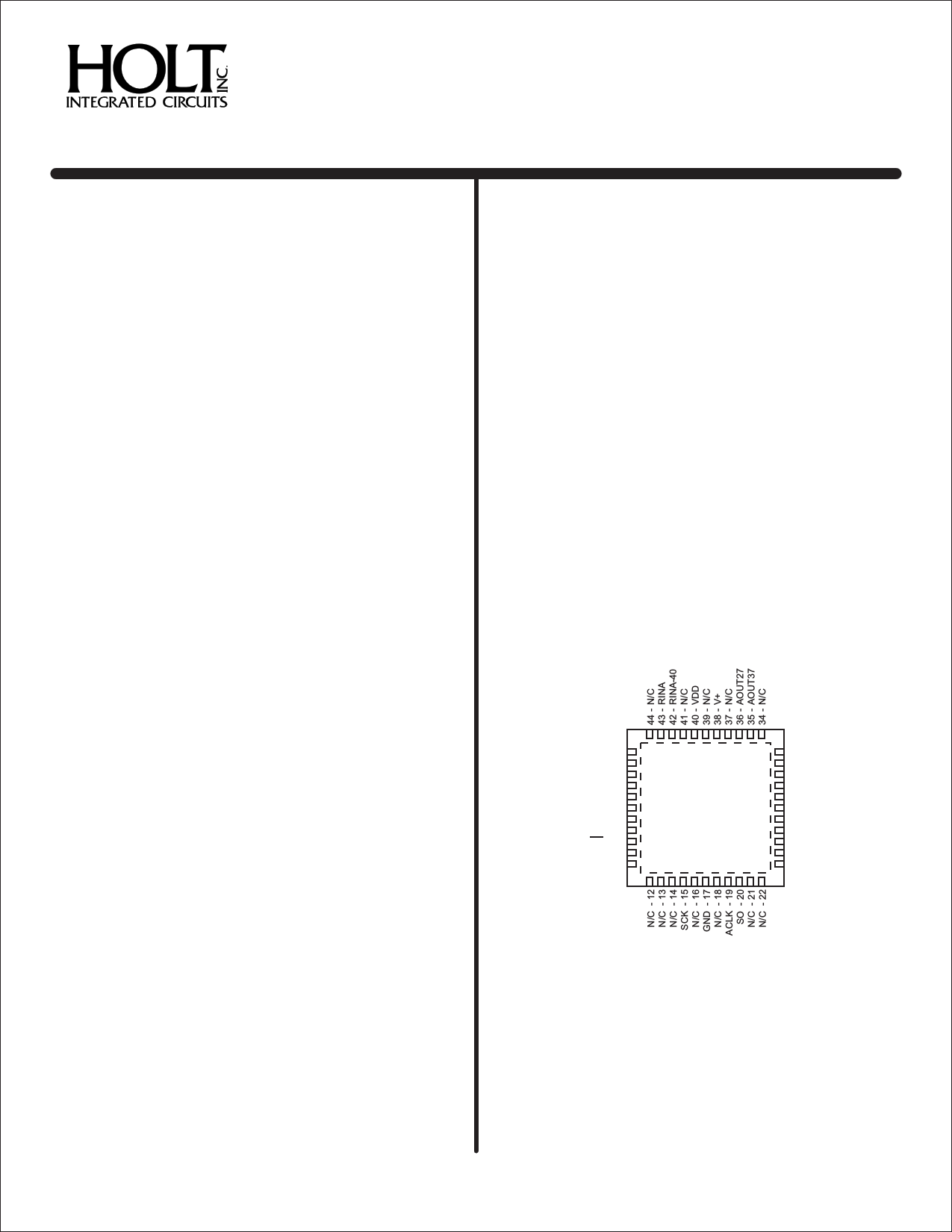
PIN CONFIGURATIONS (Top View)
N/C - 1
RINB-40 - 2
RINB - 3
N/C - 4
N/C - 5
N/C - 6
MR - 7
SI - 8
CS - 9
N/C - 10
N/C - 11
HI-3585PCI
HI-3585PCT
33 - BOUT27
32 - BOUT37
31 - N/C
30 - V-
29 - N/C
28 - TFLAG
27 - N/C
26 - N/C
25 - RFLAG
24 - N/C
23 - N/C
44 - Pin Plastic 7mm x 7mm
Chip-Scale Package (QFN)
(DS3585 Rev. N)
HOLT INTEGRATED CIRCUITS
www.holtic.com
11/15
1 page 
HI-3585, HI-3586
FUNCTIONAL DESCRIPTION (cont.)
ARINC 429 DATA FORMAT
Control Register bit CR11 controls how individual bits in the
received or transmitted ARINC word are mapped to the HI-3585 SPI
data word bits during data read or write operations. The following
table describes this mapping:
SPI
Order
1
. ARINC bit 32
Table 2. SPI / ARINC bit-mapping
2 - 22
23 24 25 26 27 28 29 30 31 32
31 - 11
10 9 1 2 3 4 5 6 7 8
CR11=0
Data
ARINC bit 32
CR11=1
31 - 11
Data
10 9 8 7 6 5 4 3 2 1
ARINC 429 RECEIVER
ARINC BUS INTERFACE
Figure 1 shows the input circuit for the on-chip ARINC 429 line
receiver. The ARINC 429 specification requires the following
detection levels:
STATE
ONE
NULL
ZERO
DIFFERENTIAL VOLTAGE
+6.5 Volts to +13 Volts
+2.5 Volts to -2.5 Volts
-6.5 Volts to -13 Volts
RINA-40
RINA
RINB
RINB-40
VDD
GND
VDD
DIFFERENTIAL
AMPLIFIERS
COMPARATORS
ONE
NULL
ZERO
GND
FIGURE 1. ARINC RECEIVER INPUT
The HI-3585 guarantees recognition of these levels with a common
mode voltage with respect to GND less than ±30V for the worst case
condition (3.15V supply and 13V signal level).
Design tolerances guarantee detection of the above levels, so the
actual acceptance ranges are slightly larger. If the ARINC signal
(including nulls) is outside the differential voltage ranges, the HI-
3585 receiver rejects the data.
RECEIVER LOGIC OPERATION
Figure 2 is a block diagram showing receiver logic.
BIT TIMING
The ARINC 429 specification defines the following timing toler-
ances for received data:
BIT RATE
PULSE RISE TIME
PULSE FALL TIME
PULSE WIDTH
HIGH SPEED
100K BPS ± 1%
1.5 ± 0.5 µsec
1.5 ± 0.5 µsec
5 µsec ± 5%
LOW SPEED
12K -14.5K BPS
10 ± 5 µsec
10 ± 5 µsec
34.5 to 41.7 µsec
The HI-3585 accepts signals within these tolerances and rejects
signals outside these tolerances. Receiver logic achieves this as
described below:
1. An accurate 1MHz clock source is required to validate the
receive signal timing. Less than 1% error is recommended.
2. The receiver uses three separate 10-bit sampling shift reg-
isters for Ones detection, Zeros detection and Null detection.
When the input signal is within the differential voltage range
for any shift register’s state (One Zero or Null) sampling
clocks a high bit into that register. When the receive signal is
outside the differential voltage range defined for any shift reg-
ister, a low bit is clocked. Only one shift register can clock a
high bit for any given sample. All three registers clock low
bits if the differential input voltage is between defined state
voltage bands.
Valid data bits require at least three consecutive One or Zero
samples (three high bits) in the upper half of the Ones or
Zeros sampling shift register, and at least three consecutive
Null samples (three high bits) in the lower half of the Null sam-
pling shift register within the data bit interval.
A word gap Null requires at least three consecutive Null sam-
ples (three high bits) in the upper half of the Null sampling
shift register and at least three consecutive Null samples
(three high bits) in the lower half of the Null sampling shift reg-
ister. This guarantees the minimum pulse width.
3. To validate the receive data bit rate, each bit must follow
its preceding bit by not less than 8 samples and not more
than 12 samples. With exactly 1MHz input clock frequency,
the acceptable data bit rates are:
DATA BIT RATE MIN
DATA BIT RATE MAX
HIGH SPEED LOW SPEED
83K BPS
125K BPS
10.4K BPS
15.6K BPS
4. Following the last data bit of a valid reception, the Word
Gap timer samples the Null shift register every 10 input
clocks (every 80 clocks for low speed). If a Null is present,
the Word Gap counter is incremented. A Word Gap count of
3 enables the next reception.
HOLT INTEGRATED CIRCUITS
5
5 Page 
HI-3585, HI-3586
HOST SERIAL PERIPHERAL INTERFACE (cont.)
HI-3585 SPI COMMANDS
For the HI-3585, each SPI read or write operation begins with an
8-bit command byte transferred from the host to the device after
assertion of CS. Since HI-3585 command byte reception is half-
duplex, the host discards the dummy byte it receives while
serially transmitting the command byte.
Figures 5 and 6 show read and write timing as it appears for a
single-byte and dual-byte register operation. The command byte
is immediately followed by a data byte comprising the 8-bit data
word read or written. For a single register read or write, CS is
negated after the data byte is transferred.
Multiple byte read or write cycles may be performed by
transferring more than one byte before CS is negated. Table 1
defines the required number of bytes for each instruction.
Note: SPI Instruction op-codes not shown in Tables 1 are
“reserved” and must not be used. Further, these op-codes will
not provide meaningful data in response to read commands.
Two instruction bytes cannot be “chained”; CS must be
negated after the command, then reasserted for the following
Read or Write command.
SCK
0 1234567 0 1234567
MSB
SI
High Z
SO
CS
LSB
Op-Code Byte
MSB
Data Byte
Figure 5. Single-Byte Read From a Register
LSB MSB
High Z
Host may continue to assert CS
here to read sequential word(s)
when allowed by the instruction.
Each word needs 8 SCK clocks.
0 1234567 0 1234567 0 1234567
SCK
SPI Mode 0
MSB
SI
LSB MSB
LSB MSB
LSB
High Z
SO
Op-Code Byte
Data Byte 0
Data Byte 1
CS
Figure 6. 2-Byte Write example
Host may continue to assert CS
here to write sequential byte(s)
when allowed by the SPI instruction.
Each byte needs 8 SCK clocks.
HOLT INTEGRATED CIRCUITS
11
11 Page | ||
| Páginas | Total 19 Páginas | |
| PDF Descargar | [ Datasheet HI-3586.PDF ] | |
Hoja de datos destacado
| Número de pieza | Descripción | Fabricantes |
| HI-3582 | 3.3V Terminal IC | HOLTIC |
| HI-3582A | 3.3V Terminal IC | HOLTIC |
| HI-3583 | 3.3V Terminal IC | HOLTIC |
| HI-3583A | 3.3V Terminal IC | HOLTIC |
| Número de pieza | Descripción | Fabricantes |
| SLA6805M | High Voltage 3 phase Motor Driver IC. |
Sanken |
| SDC1742 | 12- and 14-Bit Hybrid Synchro / Resolver-to-Digital Converters. |
Analog Devices |
|
DataSheet.es es una pagina web que funciona como un repositorio de manuales o hoja de datos de muchos de los productos más populares, |
| DataSheet.es | 2020 | Privacy Policy | Contacto | Buscar |