|
|
|
PDF AD8041 Data sheet ( Hoja de datos )
| Número de pieza | AD8041 | |
| Descripción | Rail-to-Rail Amplifier | |
| Fabricantes | Analog Devices | |
| Logotipo | ||
Hay una vista previa y un enlace de descarga de AD8041 (archivo pdf) en la parte inferior de esta página. Total 17 Páginas | ||
|
No Preview Available !
160 MHz Rail-to-Rail
Amplifier with Disable
AD8041
FEATURES
Fully Specified for +3 V, +5 V, and ؎5 V Supplies
Output Swings Rail to Rail
Input Voltage Range Extends 200 mV Below Ground
No Phase Reversal with Inputs 1 V Beyond Supplies
Disable/Power-Down Capability
Low Power of 5.2 mA (26 mW on 5 V)
High Speed and Fast Settling on 5 V:
160 MHz –3 dB Bandwidth (G = +1)
160 V/s Slew Rate
30 ns Settling Time to 0.1%
Good Video Specifications (RL = 150 ⍀, G = +2)
Gain Flatness of 0.1 dB to 30 MHz
0.03% Differential Gain Error
0.03؇ Differential Phase Error
Low Distortion
–69 dBc Worst Harmonic @ 10 MHz
Outstanding Load Drive Capability
Drives 50 mA 0.5 V from Supply Rails
Cap Load Drive of 45 pF
APPLICATIONS
Power Sensitive High Speed Systems
Video Switchers
Distribution Amplifiers
A/D Drivers
Professional Cameras
CCD Imaging Systems
Ultrasound Equipment (Multichannel)
Single-Supply Multiplexer
PRODUCT DESCRIPTION
The AD8041 is a low power voltage feedback, high speed ampli-
fier designed to operate on +3 V, +5 V, or ± 5 V supplies. It has
true single-supply capability with an input voltage range extending
200 mV below the negative rail and within 1 V of the positive rail.
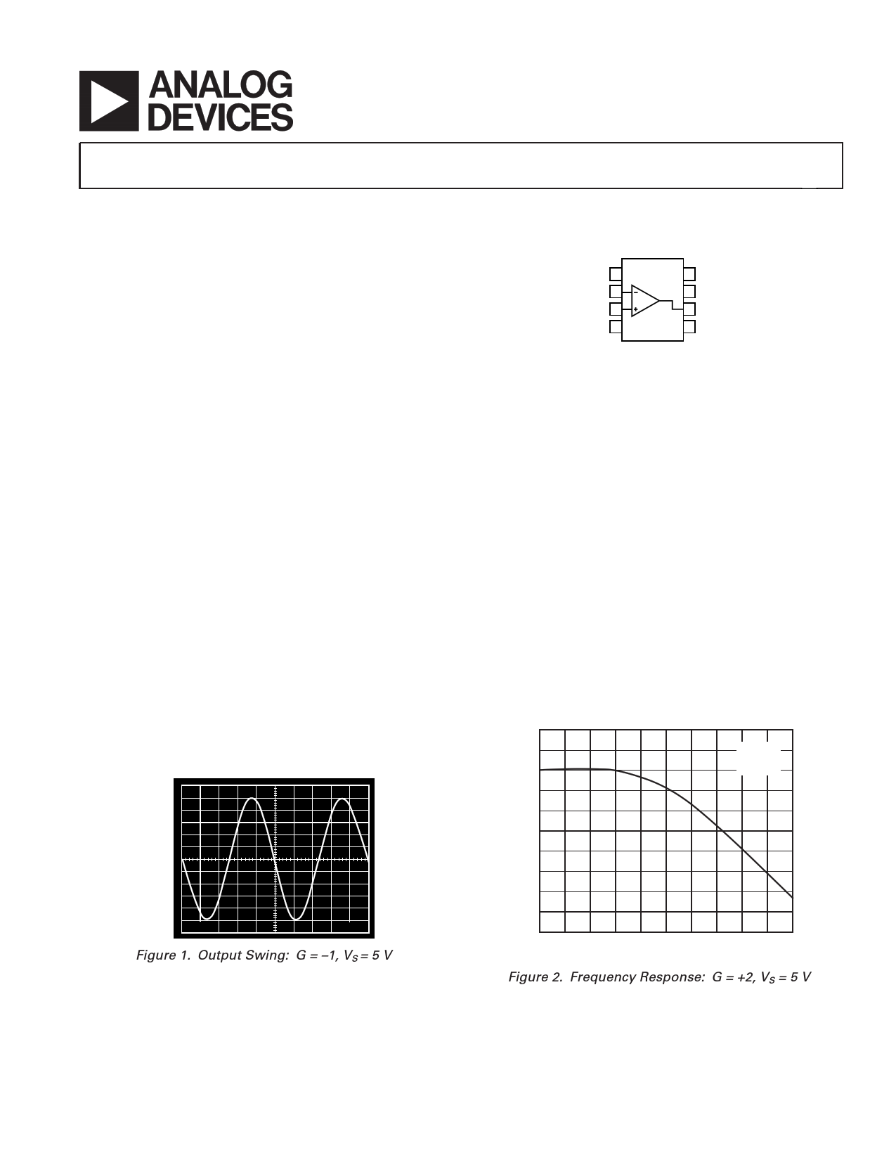
5V
2.5V
0V 1V
200ns
Figure 1. Output Swing: G = –1, VS = 5 V
REV. B
CONNECTION DIAGRAM
8-Lead PDIP, CERDIP and SOIC
NC 1
8 DISABLE
–INPUT 2
؉INPUT 3
–VS 4
AD8041
(Top View)
7 ؉VS
6 OUTPUT
5 NC
NC = NO CONNECT
The output voltage swing extends to within 50 mV of each rail,
providing the maximum output dynamic range. Additionally, it
features gain flatness of 0.1 dB to 30 MHz while offering differ-
ential gain and phase error of 0.03% and 0.03° on a single 5 V
supply. This makes the AD8041 ideal for professional video
electronics such as cameras, video switchers, or any high speed
portable equipment. The AD8041’s low distortion and fast settling
make it ideal for buffering high speed A-to-D converters.
The AD8041 has a high speed disable feature useful for mul-
tiplexing or for reducing power consumption (1.5 mA). The
disable logic interface is compatible with CMOS or open-
collector logic. The AD8041 offers a low power supply current
of 5.8 mA maximum and can run on a single 3 V power supply.
These features are ideally suited for portable and battery-
powered applications where size and power are critical.
The wide bandwidth of 160 MHz along with 160 V/µs of slew
rate on a single 5 V supply make the AD8041 useful in many
general-purpose high speed applications where dual power
supplies of up to ± 6 V and single supplies from 3 V to 12 V are
needed. The AD8041 is available in 8-lead PDIP and SOIC
over the industrial temperature range of –40°C to +85°C.
2
1 VS = 5V
G = +2
0 RF = 400⍀
–1
–2
–3
–4
–5
–6
–7
–8
0 20 40 60 80 100
FREQUENCY (MHz)
Figure 2. Frequency Response: G = +2, VS = 5 V
Information furnished by Analog Devices is believed to be accurate and
reliable. However, no responsibility is assumed by Analog Devices for its
use, nor for any infringements of patents or other rights of third parties that
may result from its use. No license is granted by implication or otherwise
under any patent or patent rights of Analog Devices. Trademarks and
registered trademarks are the property of their respective companies.
One Technology Way, P.O. Box 9106, Norwood, MA 02062-9106, U.S.A.
Tel: 781/329-4700
www.analog.com
Fax: 781/326-8703 © 2003 Analog Devices, Inc. All rights reserved.
1 page 
AD8041
SPECIFICATIONS (@ TA = 25؇C, VS = ؎5 V, RL = 2 k⍀ to 0 V, unless otherwise noted.)
Parameter
DYNAMIC PERFORMANCE
–3 dB Small Signal Bandwidth, VO < 0.5 V p-p
Bandwidth for 0.1 dB Flatness
Slew Rate
Full Power Response
Settling Time to 0.1%
Settling Time to 0.01%
NOISE/DISTORTION PERFORMANCE
Total Harmonic Distortion
Input Voltage Noise
Input Current Noise
Differential Gain Error (NTSC)
Differential Phase Error (NTSC)
DC PERFORMANCE
Input Offset Voltage
Offset Drift
Input Bias Current
Input Offset Current
Open-Loop Gain
INPUT CHARACTERISTICS
Input Resistance
Input Capacitance
Input Common-Mode Voltage Range
Common-Mode Rejection Ratio
OUTPUT CHARACTERISTICS
Output Voltage Swing: RL = 10 kΩ
Output Voltage Swing: RL = 1 kΩ
Output Voltage Swing: RL = 50 Ω
Output Current
Short-Circuit Current
Capacitive Load Drive
POWER SUPPLY
Operating Range
Quiescent Current
Quiescent Current (Disabled)
Power Supply Rejection Ratio
DISABLE CHARACTERISTICS
Turn-Off Time
Turn-On Time
Off Isolation (Pin 8 Tied to –VS)
Off Voltage (Device Disabled)
On Voltage (Device Enabled)
Specifications subject to change without notice.
Conditions
AD8041A
Min Typ Max
G = +1
G = +2, RL = 150 Ω
G = –1, VO = 2 V Step
VO = 2 V p-p
G = –1, VO = 2 V Step
140 170
32
140 170
26
30
50
fC = 5 MHz, VO = 2 V p-p, G = +2, RL = 1 kΩ
f = 10 kHz
f = 10 kHz
G = +2, RL = 150 Ω
G = +2, RL = 75 Ω
G = +2, RL = 150 Ω
G = +2, RL = 75 Ω
–77
16
600
0.02
0.02
0.03
0.10
TMIN to TMAX
TMIN to TMAX
RL = 1 kΩ
TMIN to TMAX
27
8
10
1.2 3.2
3.5
0.2 0.6
90 99
95
VCM = –5 V to +3.5 V
160
1.8
–5.2 to +4
72 80
VOUT = –4.5 V to +4.5 V
Sourcing
Sinking
G = +1
–4.45 to +4.6
–4.3 to +3.2
–4.95 to +4.95
–4.8 to +4.8
–4.5 to +3.8
50
100
160
50
3
VS = –5 V, +5 V, ± 1 V
VO = 2 V p-p @ 10 MHz, G = +2
RF = 2 kΩ
RF = 2 kΩ
RL = 100 Ω, f = 5 MHz, G = +2, RF = 1 kΩ
68
12
5.8 6.5
1.6 2.2
80
120
320
70
<VS – 2.5
Open or +VS
Unit
MHz
MHz
V/µs
MHz
ns
ns
dB
nV/√Hz
fA/√Hz
%
%
Degrees
Degrees
mV
mV
µV/°C
µA
µA
µA
dB
dB
kΩ
pF
V
dB
V
V
V
mA
mA
mA
pF
V
mA
mA
dB
ns
ns
dB
V
V
–4– REV. B
5 Page 
AD8041
5V
4V
3V
2V
1V
1V
0V
4.840V MAX
RL = 150⍀ TO 2.5V
0.111V MIN
a.
200s
5V
4.741V MAX
4V
RL = 150⍀ TO GND
3V
2V
1V
1V
0V
0.043V MIN
200s
b.
TPC 25. Output Swing vs. Load Reference Voltage,
VS = 5 V, G = –1
4.5V
3.5V
2.5V
VS = 5V
G = +2
RL = 2k⍀
VIN = 1V p-p
1.5V
0.5V
1V
40ns
TPC 26. One Volt Step Response, VS = 5 V, G = +2
2.60V
2.55V
2.50V
VS = 5V
G = +1
RL = 2k⍀
VL = 5pF
2.45V
2.40V
50mV
40ns
TPC 27. 100 mV Step Response, VS = 5 V, G = +1
3.0V
2.5V
2.0V
1.5V
1.0V
0.5V
0V
500mV
VIN = 3V p-p
f = 0.1MHz
RL = 2k⍀
VS = 3V
G = –1
2s
TPC 28. Output Swing, VS = 3 V, VIN = 3 V p-p
3.0V
2.5V
2.0V
1.5V
VIN = 2.8V p-p
f = 0.8MHz
RL = 2k⍀
VS = 3V
G = –1
1.0V
0.5V
0V
500mV
2s
TPC 29. Output Swing, VS = 3 V, VIN = 2.8 V p-p
–10–
REV. B
11 Page | ||
| Páginas | Total 17 Páginas | |
| PDF Descargar | [ Datasheet AD8041.PDF ] | |
Hoja de datos destacado
| Número de pieza | Descripción | Fabricantes |
| AD8040 | Rail-to-Rail Input/Output Amplifier | Analog Devices |
| AD8041 | Rail-to-Rail Amplifier | Analog Devices |
| AD8042 | Dual 160 MHz Rail-to-Rail Amplifier | Analog Devices |
| AD8044 | Quad 150 MHz Rail-to-Rail Amplifier | Analog Devices |
| Número de pieza | Descripción | Fabricantes |
| SLA6805M | High Voltage 3 phase Motor Driver IC. |
Sanken |
| SDC1742 | 12- and 14-Bit Hybrid Synchro / Resolver-to-Digital Converters. |
Analog Devices |
|
DataSheet.es es una pagina web que funciona como un repositorio de manuales o hoja de datos de muchos de los productos más populares, |
| DataSheet.es | 2020 | Privacy Policy | Contacto | Buscar |