|
|
|
PDF AD8079 Data sheet ( Hoja de datos )
| Número de pieza | AD8079 | |
| Descripción | Dual 260 MHz Gain = +2.0 & +2.2 Buffer | |
| Fabricantes | Analog Devices | |
| Logotipo | ||
Hay una vista previa y un enlace de descarga de AD8079 (archivo pdf) en la parte inferior de esta página. Total 13 Páginas | ||
|
No Preview Available !
a
Dual 260 MHz
Gain = +2.0 & +2.2 Buffer
AD8079
FEATURES
Factory Set Gain
AD8079A: Gain = +2.0 (Also +1.0 & –1.0)
AD8079B: Gain = +2.2 (Also +1 & –1.2)
Gain of 2.2 Compensates for System Gain Loss
Minimizes External Components
Tight Control of Gain and Gain Matching (0.1%)
Optimum Dual Pinout
Simplifies PCB Layout
Low Crosstalk of –70 dB @ 5 MHz
Excellent Video Specifications (RL = 150 ⍀)
Gain Flatness 0.1 dB to 50 MHz
0.01% Differential Gain Error
0.02؇ Differential Phase Error
Low Power of 50 mW/Amplifier (5 mA)
High Speed and Fast Settling
260 MHz, –3 dB Bandwidth
750 V/s Slew Rate (2 V Step), 800 V/s (4 V Step)
40 ns Settling Time to 0.1% (2 V Step)
Low Distortion of –65 dBc THD, fC = 5 MHz
High Output Drive of Over 70 mA
Drives Up to 8 Back-Terminated 75 ⍀ Loads (4 Loads/
Side) While Maintaining Good Differential Gain/
Phase Performance (0.01%/0.17؇)
High ESD Tolerance (5 kV)
Available in Small 8-Pin SOIC
APPLICATIONS
Differential A-to-D Driver
Video Line Driver
Differential Line Driver
Professional Cameras
Video Switchers
Special Effects
RF Receivers
PRODUCT DESCRIPTION
The AD8079 is a dual, low power, high speed buffer designed
to operate on ± 5 V supplies. The AD8079’s pinout offers excel-
lent input and output isolation compared to the traditional dual
amplifier pin configuration. With two ac ground pins separating
both the inputs and outputs, the AD8079 achieves very low
crosstalk of less than –70 dB at 5 MHz.
Additionally, the AD8079 contains gain setting resistors factory
set at G = +2.0 (A grade) or Gain = +2.2 (B grade) allowing
circuit configurations with minimal external components. The
B grade gain of +2.2 compensates for gain loss through a system
by providing a single-point trim. Using active laser trimming of
these resistors, the AD8079 guarantees tight control of gain and
channel-channel gain matching. With its performance and con-
figuration, the AD8079 is well suited for driving differential
REV. A
Information furnished by Analog Devices is believed to be accurate and
reliable. However, no responsibility is assumed by Analog Devices for its
use, nor for any infringements of patents or other rights of third parties
which may result from its use. No license is granted by implication or
otherwise under any patent or patent rights of Analog Devices.
FUNCTIONAL BLOCK DIAGRAM
8-Pin Plastic SOIC
+IN1 1
GND 2
GND 3
AD8079
+IN2 4
8 OUT1
7 +VS
6 –VS
5 OUT2
cables and transformers. Its low distortion and fast settling are
ideal for buffering high speed dual or differential A-to-D con-
verters.
The AD8079 features a unique transimpedance linearization
circuitry. This allows it to drive video loads with excellent differ-
ential gain and phase performance of 0.01% and 0.02° on only
50 mW of power per amplifier. It features gain flatness of 0.1 dB
to 50 MHz. This makes the AD8079 ideal for professional video
electronics such as cameras and video switchers.
The AD8079 offers low power of 5 mA/amplifier (VS = ± 5 V)
and can run on a single +12 V power supply while delivering
over 70 mA of load current. All of this is offered in a small 8-pin
SOIC package. These features make this amplifier ideal for por-
table and battery powered applications where size and power are
critical.
The outstanding bandwidth of 260 MHz along with 800 V/µs of
slew rate make the AD8079 useful in many general purpose high
speed applications where dual power supplies of ± 3 V to ± 6 V
are required.
The AD8079 is available in the industrial temperature range of
–40°C to +85°C.
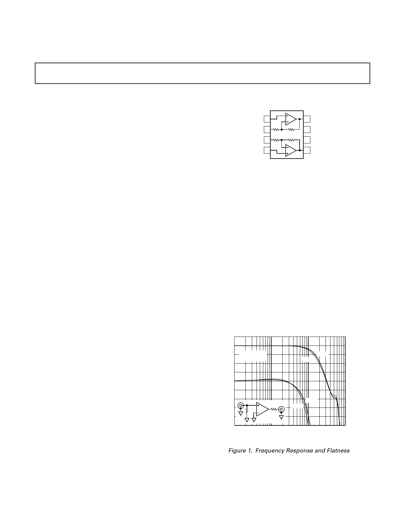
1
RL = 100Ω
VIN = 50mV rms
SIDE 2
SIDE 1
0
–1
–2
0.1 –3
0 –4
–0.1
–5
–0.2
–0.3
–0.4
SIDE 2
50Ω SIDE 1
50Ω
–6
–7
–8
–0.5
1M
10M
100M
FREQUENCY – Hz
–9
1G
Figure 1. Frequency Response and Flatness
One Technology Way, P.O. Box 9106, Norwood, MA 02062-9106, U.S.A.
Tel: 617/329-4700 World Wide Web Site: http://www.analog.com
Fax: 617/326-8703
© Analog Devices, Inc., 1996
1 page 
AD8079
+5V 10µF
0.1µF
VIN
PULSE
GENERATOR
27
AD8079 8
1
50Ω
0.1µF
6
10µF
TR/TF = 250ps
–5V
RL = 100Ω
Figure 3. Test Circuit
SIDE 1
100mV STEP
SIDE 2
20mV
5ns
Figure 4. 100 mV Step Response
SIDE 1
1V STEP
SIDE 2
200mV
5ns
Figure 5. 1 V Step Response
RL = 100Ω
VIN = 50mV rms
SIDE 2
SIDE 1
0.1
0
–0.1
–0.2
–0.3
–0.4
SIDE 2
50Ω SIDE 1
50Ω
–0.5
1M
10M
100M
FREQUENCY – Hz
1
0
–1
–2
–3
–4
–5
–6
–7
–8
–9
1G
Figure 6. Frequency Response and Flatness
–50
RL = 100Ω
–60
–70
2ND HARMONIC
–80
3RD HARMONIC
–90
–100
–110
10k
100k
1M
FREQUENCY – Hz
10M
100M
Figure 7. Distortion vs. Frequency, RL = 100 Ω
–60
RL = 1kΩ
VOUT = 2Vp-p
–70
–80
–90
–100
2ND HARMONIC
3RD HARMONIC
–110
–120
10k
100k
1M 10M
FREQUENCY – Hz
100M
Figure 8. Distortion vs. Frequency, RL = 1 kΩ
–4– REV. A
5 Page 
AD8079
+VS
IN
RT
50Ω
OUT
–VS
Inverting Configuration
+VS
C1 C3
0.1µF
10µF
C2
0.1µF
C4
10µF
–VS
Supply Bypassing
+VS
50Ω
OUT
IN
RT –VS
*SEE TABLE I
Noninverting Configuration (G = +2)
TRIM
200Ω AD8079B
IN
RT
OUT
Optional Gain Trim (G = +2 → +2.2)
TIE INPUT PINS
TOGETHER
TO MINIMIZE
PEAKING
+VS
IN
RT –VS
OUT
Noninverting Configuration (G = +1)
Figure 29. Inverting and Noninverting Configurations
Table I. Recommended Component Values
Component
RT (Nominal) (Ω)
Small Signal BW (MHz)
0.1 dB Flatness (MHz)
–1
53.6
220
50
+1
49.9
750
100
+2/+2.2
49.9
260
50
Figure 30. Board Layout (Silkscreen)
Figure 31. Board Layout (Component Layer)
Figure 32. Board Layout (Solder Side; Looking Through
the Board)
–10–
REV. A
11 Page | ||
| Páginas | Total 13 Páginas | |
| PDF Descargar | [ Datasheet AD8079.PDF ] | |
Hoja de datos destacado
| Número de pieza | Descripción | Fabricantes |
| AD807 | Fiber Optic Receiver | Analog Devices |
| AD8072 | Dual/Triple Video Amplifiers | Analog Devices |
| AD8073 | Dual/Triple Video Amplifiers | Analog Devices |
| AD8074 | G = +1 and +2 Triple Video Buffers | Analog Devices |
| Número de pieza | Descripción | Fabricantes |
| SLA6805M | High Voltage 3 phase Motor Driver IC. |
Sanken |
| SDC1742 | 12- and 14-Bit Hybrid Synchro / Resolver-to-Digital Converters. |
Analog Devices |
|
DataSheet.es es una pagina web que funciona como un repositorio de manuales o hoja de datos de muchos de los productos más populares, |
| DataSheet.es | 2020 | Privacy Policy | Contacto | Buscar |