|
|
PDF CD4047BMS Data sheet ( Hoja de datos )
| Número de pieza | CD4047BMS | |
| Descripción | CMOS Low-Power Monostable/Astable Multivibrator | |
| Fabricantes | Intersil Corporation | |
| Logotipo |  |
|
Hay una vista previa y un enlace de descarga de CD4047BMS (archivo pdf) en la parte inferior de esta página. Total 15 Páginas | ||
|
No Preview Available !
CD4047BMS
December 1992
CMOS Low-Power
Monostable/Astable Multivibrator
Features
• High Voltage Type (20V Rating)
• Low Power Consumption: Special CMOS Oscillator
Configuration
• Monostable (One-Shot) or Astable (Free-Running)
Operation
• True and Complemented Buffered Outputs
• Only One External R and C Required
• Buffered Inputs
• 100% Tested for Quiescent Current at 20V
• Standardized, Symmetrical Output Characteristics
• 5V, 10V and 15V Parametric Ratings
• Meets All Requirements of JEDEC Tentative Standard
No. 13B, “Standard Specifications for Description of
‘B’ Series CMOS Devices”
Monostable Multivibrator Features
• Positive or Negative Edge Trigger
• Output Pulse Width Independent of Trigger Pulse
Duration
• Retriggerable Option for Pulse Width Expansion
• Internal Power-On Reset Circuit
• Long Pulse Widths Possible Using Small RC Compo-
nents by Means of External Counter Provision
• Fast Recovery Time Essentially Independent of Pulse
Width
• Pulse-Width Accuracy Maintained at Duty Cycles
Approaching 100%
Astable Multivibrator Features
• Free-Running or Gatable Operating Modes
• 50% Duty Cycle
• Oscillator Output Available
• Good Astable Frequency Stability: Frequency Deviation:
- = ±2% + 0.03%/oC at 100kHz
- = ±0.5% + 0.015%/oC at 10kHz (Circuits “Trimmed”
to Frequency VDD = 10V ± 10%
Applications
Digital equipment where low power dissipation and/or high noise
immunity are primary design requirements
• Envelope Detection
• Frequency Discriminators
• Frequency Multiplication • Timing Circuits
• Frequency Division
• Time Delay Applications
Description
CD4047BMS consists of a gatable astable multivibrator with logic tech-
niques incorporated to permit positive or negative edge triggered
monostable multivibrator action with retriggering and external counting
options.
Inputs include +TRIGGER, -TRIGGER, ASTABLE, ASTABLE,
RETRIGGER, and EXTERNAL RESET. Buffered outputs are Q, Q, and
OSCILLATOR. In all modes of operation, an external capacitor must be
connected between C-Timing and RC-Common terminals, and an
external resistor must be connected between the R-Timing and RC-
Common terminals.
Astable operation is enabled by a high level on the ASTABLE input or a
low level on the ASTABLE input, or both. The period of the square wave
at the Q and Q Outputs in this mode of operation is a function of the
external components employed. “True” input pulses on the ASTABLE
input or “Complement” pulses on the ASTABLE input allow the circuit to
be used as a gatable multivibrator. The OSCILLATOR output period will
be half of the Q terminal output in the astable mode. However, a 50%
duty cycle is not guaranteed at this output.
The CD4047BMS triggers in the monostable mode when a positive
going edge occurs on the +TRIGGER input while the -TRIGGER is held
low. Input pulses may be of any duration relative to the output pulse.
If retrigger capability is desired, the RETRIGGER input is pulsed. The
retriggerable mode of operation is limited to positive going edge. The
CD4047BMS will retrigger as long as the RETRIGGER input is high,
with or without transitions (See Figure 31)
An external countdown option can be implemented by coupling “Q” to
an external “N” counter and resetting the counter with trigger pulse. The
counter output pulse is fed back to the ASTABLE input and has a dura-
tion equal to N times the period of the multivibrator.
A high level on the EXTERNAL RESET input assures no output pulse
during an “ON” power condition. This input can also be activated to ter-
minate the output pulse at any time. For monostable operation, when-
ever VDD is applied, an internal power on reset circuit will clock the Q
output low within one output period (tM).
The CD4047BMS is supplied in these 14-lead outline packages:
Braze Seal DIP H4Q
Frit Seal DIP
H1B
Ceramic Flatpack H3W
Pinout
CD4047BMS
TOP VIEW
C1
R2
R-C COMMON 3
ASTABLE 4
ASTABLE 5
-TRIGGER 6
VSS 7
14 VDD
13 OSC OUT
12 RETRIGGER
11 Q
10 Q
9 EXT. RESET
8 +TRIGGER
CAUTION: These devices are sensitive to electrostatic discharge; follow proper IC Handling Procedures.
1-888-INTERSIL or 321-724-7143 | Copyright © Intersil Corporation 1999
7-897
File Number 3313
1 page 
Specifications CD4047BMS
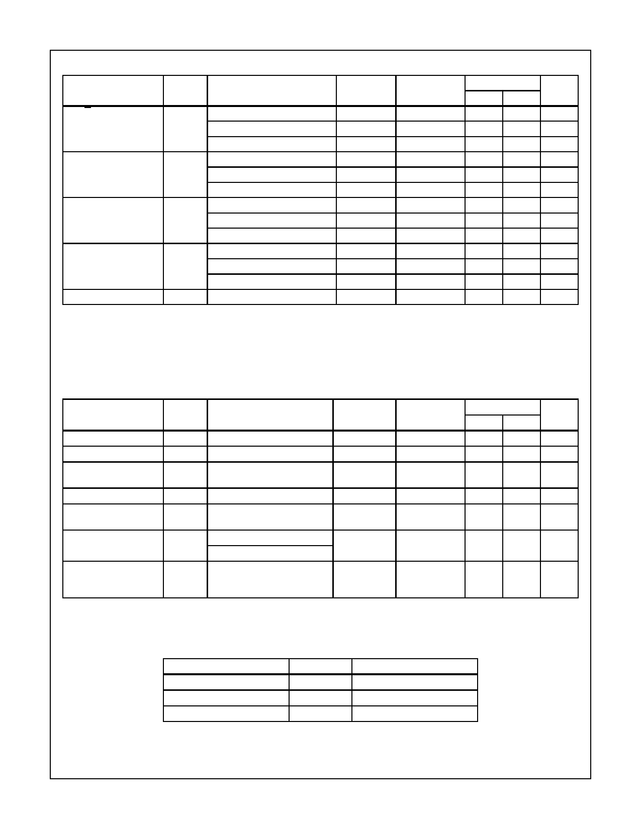
TABLE 3. ELECTRICAL PERFORMANCE CHARACTERISTICS (Continued)
LIMITS
PARAMETER
SYMBOL
CONDITIONS
Q or Q Deviation from
50% Duty Factor
QD VDD = 5V
VDD = 10V
VDD = 15V
Minimum Pulse Width
+ Trigger
- Trigger
TW VDD = 5V
VDD = 10V
VDD = 15V
Minimum Pulse Width
Reset
TW VDD = 5V
VDD = 10V
VDD = 15V
Minimum Retrigger Pulse
Width
TW VDD = 5V
VDD = 10V
VDD = 15V
Input Capacitance
CIN Any Input
NOTES
1, 2, 3
1, 2, 3
1, 2, 3
1, 2, 3
1, 2, 3
1, 2, 3
1, 2, 3
1, 2, 3
1, 2, 3
1, 2, 3
1, 2, 3
1, 2, 3
1, 2
TEMPERATURE
+25oC
+25oC
+25oC
+25oC
+25oC
+25oC
+25oC
+25oC
+25oC
+25oC
+25oC
+25oC
+25oC
MIN
-
-
-
-
-
-
-
-
-
-
-
-
-
MAX
±1
±1
±0.5
400
160
100
200
100
60
600
230
150
7.7
UNITS
%
%
%
ns
ns
ns
ns
ns
ns
ns
ns
ns
pF
NOTES:
1. All voltages referenced to device GND.
2. The parameters listed on Table 3 are controlled via design or process and are not directly tested. These parameters are characterized
on initial design release and upon design changes which would affect these characteristics.
3. CL = 50pF, RL = 200K, Input TR, TF < 20ns.
TABLE 4. POST IRRADIATION ELECTRICAL PERFORMANCE CHARACTERISTICS
LIMITS
PARAMETER
Supply Current
N Threshold Voltage
N Threshold Voltage
Delta
P Threshold Voltage
P Threshold Voltage
Delta
Functional
Propagation Delay Time
SYMBOL
CONDITIONS
IDD VDD = 20V, VIN = VDD or GND
VNTH VDD = 10V, ISS = -10µA
∆VTN VDD = 10V, ISS = -10µA
VTP
∆VTP
VSS = 0V, IDD = 10µA
VSS = 0V, IDD = 10µA
F
TPHL
TPLH
VDD = 18V, VIN = VDD or GND
VDD = 3V, VIN = VDD or GND
VDD = 5V
NOTES: 1. All voltages referenced to device GND.
2. CL = 50pF, RL = 200K, Input TR, TF < 20ns.
NOTES
1, 4
1, 4
1, 4
TEMPERATURE
+25oC
+25oC
+25oC
MIN
-
-2.8
-
1, 4
+25oC
0.2
1, 4
+25oC
-
1
1, 2, 3, 4
+25oC
+25oC
VOH >
VDD/2
-
3. See Table 2 for +25oC limit.
4. Read and Record
MAX
7.5
-0.2
±1
2.8
±1
VOL <
VDD/2
1.35 x
+25oC
Limit
UNITS
µA
V
V
V
V
V
ns
TABLE 5. BURN-IN AND LIFE TEST DELTA PARAMETERS +25OC
PARAMETER
SYMBOL
DELTA LIMIT
Supply Current - MSI-1
Output Current (Sink)
Output Current (Source)
IDD
IOL5
IOH5A
± 0.2µA
± 20% x Pre-Test Reading
± 20% x Pre-Test Reading
7-901
5 Page 
CD4047BMS
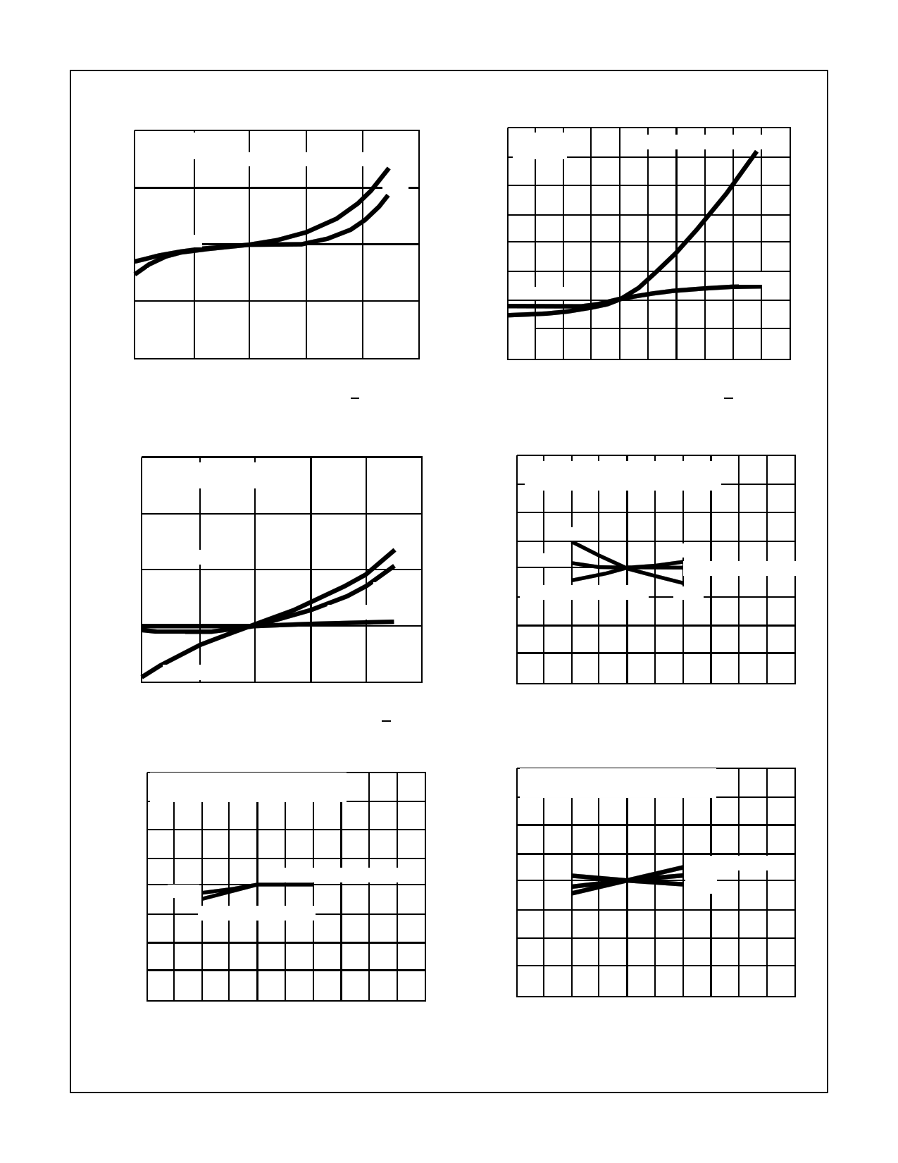
Typical Performance Characteristics (Continued)
2
CX = 0.01µF
RX = 100kΩ
1
SUPPLY VOLTAGE (VDD) = 5V, 10V
15V
0 5V AND 10V
12
CX = 1000pF
10 RX = 10kΩ
8
6
4
SUPPLY VOLTAGE (VDD) = 5V
15V
-1
2
0 10V AND 15V
-2 5V
10V, 15V
-2
-55
-15 25 65 105
AMBIENT TEMPERATURE (TA) (oC)
145
FIGURE 16. TYP. ASTABLE OSCILLATOR OR Q, Q PERIOD
ACCURACY vs AMBIENT TEMPERATURE (MEDIUM
FREQ.)
RX = 10kΩ
SUPPLY VOLTAGE (VDD) = 5V
-4
-55 -35 -15 -5 25 45 65 85 105 125 145
AMBIENT TEMPERATURE (TA) (oC)
FIGURE 17. TYP. ASTABLE OSCILLATOR OR Q, Q PERIOD
ACCURACY vs AMBIENT TEMPERATURE (HIGH
FREQ.)
8
AMBIENT TEMPERATURE (TA) = +25oC
6 CX = 1µF
20
100pF
10
0.01µF, 0.1µF, 1µF
0
0.001µF
0.001µF
0.01µF, 0.1µF, 1µF
-10 CX = 100pF
-55 -15 25 65 105 145
AMBIENT TEMPERATURE (TA) (oC)
FIGURE 18. TYPICAL ASTABLE OSCILLATOR OR Q, Q PERIOD
ACCURACY vs AMBIENT TEMPERATURE
4
2 1kΩ
0 10kΩ
-2 RX = 100kΩ, 1MΩ, 10MΩ
100kΩ
10kΩ, 1MΩ AND 10MΩ
1kΩ
-4
-6
-8
0
5 10 15 20
SUPPLY VOLTAGE (VDD) (V)
25
FIGURE 19. TYPICAL OUTPUT PULSE WIDTH VARIATIONS vs
SUPPLY VOLTAGE
8 AMBIENT TEMPERATURE (TA) = +25oC
6 CX = 0.1µF
4
2
0
10MΩ
10kΩ, 100kΩ, 1MΩ AND 10MΩ
-2 RX = 10kΩ, 100kΩ, 1MΩ
-4
-6
-8
0
5 10 15 20
SUPPLY VOLTAGE (VDD) (V)
25
FIGURE 20. TYPICAL OUTPUT PULSE WIDTH VARIATIONS vs
SUPPLY VOLTAGE
8 AMBIENT TEMPERATURE (TA) = +25oC
6 CX = 1000pF
4
2
RX = 1MΩ AND 10Ω
0 100kΩ
10kΩ
-2
-4
-6
-8
0
5 10 15 20
SUPPLY VOLTAGE (VDD) (V)
25
FIGURE 21. TYPICAL OUTPUT PULSE WIDTH VARIATIONS vs
SUPPLY VOLTAGE
7-907
11 Page | ||
| Páginas | Total 15 Páginas | |
| PDF Descargar | [ Datasheet CD4047BMS.PDF ] | |
Hoja de datos destacado
| Número de pieza | Descripción | Fabricantes |
| CD4047BM | Low Power Monostable/Astable Multivibrator | National Semiconductor |
| CD4047BMS | CMOS Low-Power Monostable/Astable Multivibrator | Intersil Corporation |
| Número de pieza | Descripción | Fabricantes |
| SLA6805M | High Voltage 3 phase Motor Driver IC. |
Sanken |
| SDC1742 | 12- and 14-Bit Hybrid Synchro / Resolver-to-Digital Converters. |
Analog Devices |
|
DataSheet.es es una pagina web que funciona como un repositorio de manuales o hoja de datos de muchos de los productos más populares, |
| DataSheet.es | 2020 | Privacy Policy | Contacto | Buscar |
