|
|
|
PDF IDT72V05 Data sheet ( Hoja de datos )
| Número de pieza | IDT72V05 | |
| Descripción | 3.3 VOLT CMOS ASYNCHRONOUS FIFO | |
| Fabricantes | Integrated Device Technology | |
| Logotipo | ||
Hay una vista previa y un enlace de descarga de IDT72V05 (archivo pdf) en la parte inferior de esta página. Total 12 Páginas | ||
|
No Preview Available !
3.3 VOLT CMOS ASYNCHRONOUS FIFO
512 x 9, 1,024 x 9,
2,048 x 9, 4,096 x 9,
8,192 x 9, 16,384 x 9
IDT72V01, IDT72V02
IDT72V03, IDT72V04
IDT72V05, IDT72V06
FEATURES:
• 3.3V family uses less power than the 5 Volt 7201/7202/7203/7204/
7205/7206 family
• 512 x 9 organization (72V01)
• 1,024 x 9 organization (72V02)
• 2,048 x 9 organization (72V03)
• 4,096 X 9 organization (72V04)
• 8,192 x 9 organization (72V05)
• 16,384 X 9 organization (72V06)
• Functionally compatible with 720x family
• Low-power consumption
— Active: 180 mW (max.)
— Power-down: 18 mW (max.)
• 15 ns access time
• Asynchronous and simultaneous read and write
• Fully expandable by both word depth and/or bit width
• Status Flags: Empty, Half-Full, Full
• Auto-retransmit capability
• Available in 32-pin PLCC
• Industrial temperature range (–40°C to +85°C) is available
• Green parts available, see ordering information
DESCRIPTION:
The IDT72V01/72V02/72V03/72V04/72V05/72V06 are dual-port FIFO
memories that operate at a power supply voltage (Vcc) between 3.0V and 3.6V.
Their architecture, functional operation and pin assignments are identical to
those of the IDT7201/7202/7203/7204/7205/7206. These devices load and
empty data on a first-in/first-out basis. They use Full and Empty flags to prevent
data overflow and underflow and expansion logic to allow for unlimited
expansion capability in both word size and depth.
The reads and writes are internally sequential through the use of ring
pointers, with no address information required to load and unload data. Data
is toggled in and out of the devices through the use of the Write (W) and Read
(R) pins. The devices have a maximum data access time as fast as 25 ns.
The devices utilize a 9-bit wide data array to allow for control and parity bits
at the user’s option. This feature is especially useful in data communications
applications where it is necessary to use a parity bit for transmission/reception
error checking. They also feature a Retransmit (RT) capability that allows for
reset of the read pointer to its initial position when RT is pulsed LOW to allow for
retransmission from the beginning of data. A Half-Full Flag is available in the
single device mode and width expansion modes.
These FIFOs are fabricated using high-speed CMOS technology. It has
been designed for those applications requiring asynchronous and simultane-
ous read/writes in multiprocessing and rate buffer applications.
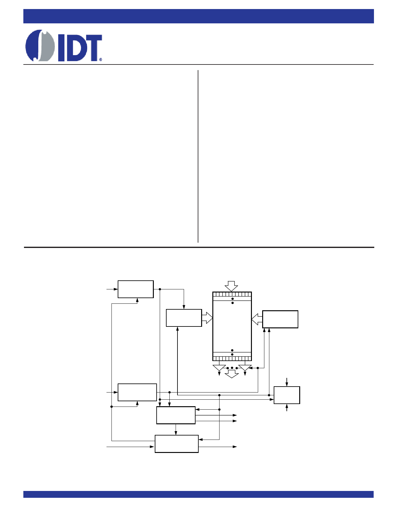
FUNCTIONAL BLOCK DIAGRAM
W
WRITE
CONTROL
DATA INPUTS
(D0-D8)
WRITE
POINTER
RAM
ARRAY
512 x 9
1,024 x 9
2,048 x 9
4,096 x 9
8,192 x 9
16,384 x 9
READ
POINTER
R
READ
CONTROL
THREE-
STATE
BUFFERS
DATA OUTPUTS
(Q0-Q8)
FLAG
LOGIC
EF
FF
RS
RESET
LOGIC
FL/RT
EXPANSION
XI
LOGIC
XO/HF
3033 drw 01
IDT and the IDT logo are trademarks of Integrated Device Technology, Inc
COMMERCIAL AND INDUSTRIAL TEMPERATURE RANGES
1
©2012 Integrated Device Technology, Inc. All rights reserved. Product specifications subject to change without notice.
JUNE 2012
DSC-3033/7
1 page 
IDT72V01/72V02/72V03/72V04/72V05/72V06 3.3V ASYNCHRONOUS FIFO
512 x 9, 1,024 x 9, 2,048 x 9, 4,096 x 9, 8,192 x 9 and 16,384 x 9
RS
W
R
EF
HF, FF
tRSC
tRS
tRSS
tRSS
tEFL
tHFH, tFFH
NOTES:
1. EF, FF, HF may change status during Reset, but flags will be valid at tRSC.
2. W and R = VIH around the rising edge of RS.
Figure 2. Reset
COMMERCIAL AND INDUSTRIAL
TEMPERATURE RANGES
tRSR
3033 drw 04
R
Q0-Q8
W
D0-D8
tRC
tA
tRR
tRPW
tA
tRLZ
tWPW
tDV
DATA OUT VALID
tWC
tWR
tRHZ
DATA OUT VALID
tDS tDH
DATA IN VALID
DATA IN VALID
Figure 3. Asynchronous Write and Read Operation
3033 drw 05
LAST WRITE
IGNORED
WRITE
FIRST READ
ADDITIONAL FIRST
READS
WRITE
R
W
tWFF
FF
t RFF
Figure 4. Full Flag From Last Write to First Read
5
3033 drw 06
5 Page 
IDT72V01/72V02/72V03/72V04/72V05/72V06 3.3V ASYNCHRONOUS FIFO
512 x 9, 1,024 x 9, 2,048 x 9, 4,096 x 9, 8,192 x 9 and 16,384 x 9
WA
FFA
DA 0-8
IDT
72V01
77I22DVVT0023
77220V10A4
72V05
72V06
RB
EFB
HFB
QB 0-8
SYSTEM A
QA 0-8
RA
HFA
EFA
IDT
72V01
72V02
72V03
72V04
72V05
72V06
DB 0-8
WB
FFB
Figure 16. Bidirectional FIFO Mode
COMMERCIAL AND INDUSTRIAL
TEMPERATURE RANGES
SYSTEM B
3033 drw 18
DATA IN
W
R
EF
DATA OUT
R
W
FF
DATA IN
DATA OUT
tRPE
tWLZ
tWEF
tA
tREF
DATA OUTVALID
Figure 17. Read Data Flow-Through Mode
3033 drw 19
tRFF
tA
DATA OUT VALID
Figure 18. Write Data Flow-Through Mode
11
tWPF
tWFF
DATA IN VALID
tDS
tDH
3033 drw 20
11 Page | ||
| Páginas | Total 12 Páginas | |
| PDF Descargar | [ Datasheet IDT72V05.PDF ] | |
Hoja de datos destacado
| Número de pieza | Descripción | Fabricantes |
| IDT72V01 | 3.3 VOLT CMOS ASYNCHRONOUS FIFO | Integrated Device Technology |
| IDT72V02 | 3.3 VOLT CMOS ASYNCHRONOUS FIFO | Integrated Device Technology |
| IDT72V03 | 3.3 VOLT CMOS ASYNCHRONOUS FIFO | Integrated Device Technology |
| IDT72V04 | 3.3 VOLT CMOS ASYNCHRONOUS FIFO | Integrated Device Technology |
| Número de pieza | Descripción | Fabricantes |
| SLA6805M | High Voltage 3 phase Motor Driver IC. |
Sanken |
| SDC1742 | 12- and 14-Bit Hybrid Synchro / Resolver-to-Digital Converters. |
Analog Devices |
|
DataSheet.es es una pagina web que funciona como un repositorio de manuales o hoja de datos de muchos de los productos más populares, |
| DataSheet.es | 2020 | Privacy Policy | Contacto | Buscar |