|
|
PDF EDD12322GBH-TS Data sheet ( Hoja de datos )
| Número de pieza | EDD12322GBH-TS | |
| Descripción | 128M bits DDR Mobile RAM | |
| Fabricantes | Elpida Memory | |
| Logotipo |  |
|
Hay una vista previa y un enlace de descarga de EDD12322GBH-TS (archivo pdf) en la parte inferior de esta página. Total 30 Páginas | ||
|
No Preview Available !
PRELIMINARY DATA SHEET
128M bits DDR Mobile RAM
WTR (Wide Temperature Range)
EDD12322GBH-TS (4M words × 32 bits)
Specifications
• Density: 128M bits
• Organization
× 32 bits: 1M words × 32 bits × 4 banks
• Package: 90-ball FBGA
Lead-free (RoHS compliant) and Halogen-free
• Power supply: VDD, VDDQ = 1.7V to 1.95V
• Data rate: 333Mbps/266Mbps (max.)
• 1KB page size
Row address: A0 to A11
Column address: A0 to A7
• Four internal banks for concurrent operation
• Interface: LVCMOS
• Burst lengths (BL): 2, 4, 8, 16
• Burst type (BT):
Sequential (2, 4, 8, 16)
Interleave (2, 4, 8, 16)
• /CAS Latency (CL): 3
• Precharge: auto precharge option for each burst
access
• Driver strength: normal, 1/2, 1/4, 1/8
• Refresh: auto-refresh, self-refresh
• Refresh cycles: 4096 cycles/64ms
Average refresh period: 15.6µs
• Operating ambient temperature range
TA = −25°C to +85°C
Features
• DLL is not implemented
• Low power consumption
• Double-data-rate architecture; two data transfers per
one clock cycle
• The high-speed data transfer is realized by the 2 bits
prefetch pipelined architecture
• Bi-directional data strobe (DQS) is transmitted
/received with data for capturing data at the receiver.
• Data inputs, outputs, and DM are synchronized with
DQS
• DQS is edge-aligned with data for READs; center-
aligned with data for WRITEs
• Differential clock inputs (CK and /CK)
• Commands entered on each positive CK edge: data
and data mask referenced to both edges of DQS
• Data mask (DM) for write data
• Burst termination by burst stop command and
Precharge command
• Wide temperature range
TA = −25°C to +85°C
Document No. E1530E20 (Ver. 2.0)
Date Published October 2009 (K) Japan
Printed in Japan
URL: http://www.elpida.com
Elpida Memory, Inc. 2009
1 page 
EDD12322GBH-TS
Electrical Specifications
• All voltages are referenced to VSS (GND).
• After power up, wait more than 200 µs and then, execute power on sequence and CBR (Auto) refresh before
proper device operation is achieved.
Absolute Maximum Ratings
Parameter
Voltage on any pin relative to VSS
Supply voltage relative to VSS
Short circuit output current
Power dissipation
Operating ambient temperature
Storage temperature
Symbol
VT
VDD
IOS
PD
TA
Tstg
Rating
–0.5 to +2.3
–0.5 to +2.3
50
1.0
–25 to +85
–55 to +125
Unit Note
V
V
mA
W
°C
°C
Caution
Exposing the device to stress above those listed in Absolute Maximum Ratings could cause
permanent damage. The device is not meant to be operated under conditions outside the limits
described in the operational section of this specification. Exposure to Absolute Maximum Rating
conditions for extended periods may affect device reliability.
Recommended DC Operating Conditions (TA = −25°C to +85°C)
Parameter
Pins
Symbol
min.
typ. max.
Unit Notes
Supply voltage
VDD,
VDDQ
VSS,
VSSQ
1.7
0
1.8 1.95
00
V1
V
Input high voltage
All other input VIH
0.8 × VDDQ
—
VDDQ + 0.3 V 2
Input low voltage
pins VIL
–0.3
— 0.2 × VDDQ V 3
DC input voltage level
CK, /CK
VIN (DC)
–0.3
—
VDDQ + 0.3
V
AC Input differential cross
point voltage
VIX
0.4 × VDDQ
0.5 × VDDQ 0.6 × VDDQ V 6
DC input differential voltage
VID (DC)
0.4 × VDDQ
—
VDDQ + 0.6 V 5
AC input differential voltage
VID (AC)
0.6 × VDDQ
—
VDDQ + 0.6 V 5
DC input high voltage
DQ, DM, DQS VIHD (DC) 0.7× VDDQ
—
VDDQ + 0.3
V
DC input low voltage
VILD (DC)
–0.3
—
0.3 × VDDQ
V
AC input high voltage
VIHD (AC) 0.8× VDDQ
—
VDDQ + 0.3
V
AC input low voltage
VILD (AC)
–0.3
—
0.2 × VDDQ
V
Notes: 1. VDDQ must be equal to VDD.
2. VIH (max.) = 2.3V (pulse width ≤ 5ns).
3. VIL (min.) = –0.5V (pulse width ≤ 5ns).
4. All voltage referred to VSS and VSSQ must be same potential.
5. VID (DC) and VID (AC) are the magnitude of the difference between the input level on CK and the input
level on /CK.
6. The value of VIX is expected to be 0.5 × VDDQ and must track variations in the DC level of the same.
Preliminary Data Sheet E1530E20 (Ver. 2.0)
5
5 Page 
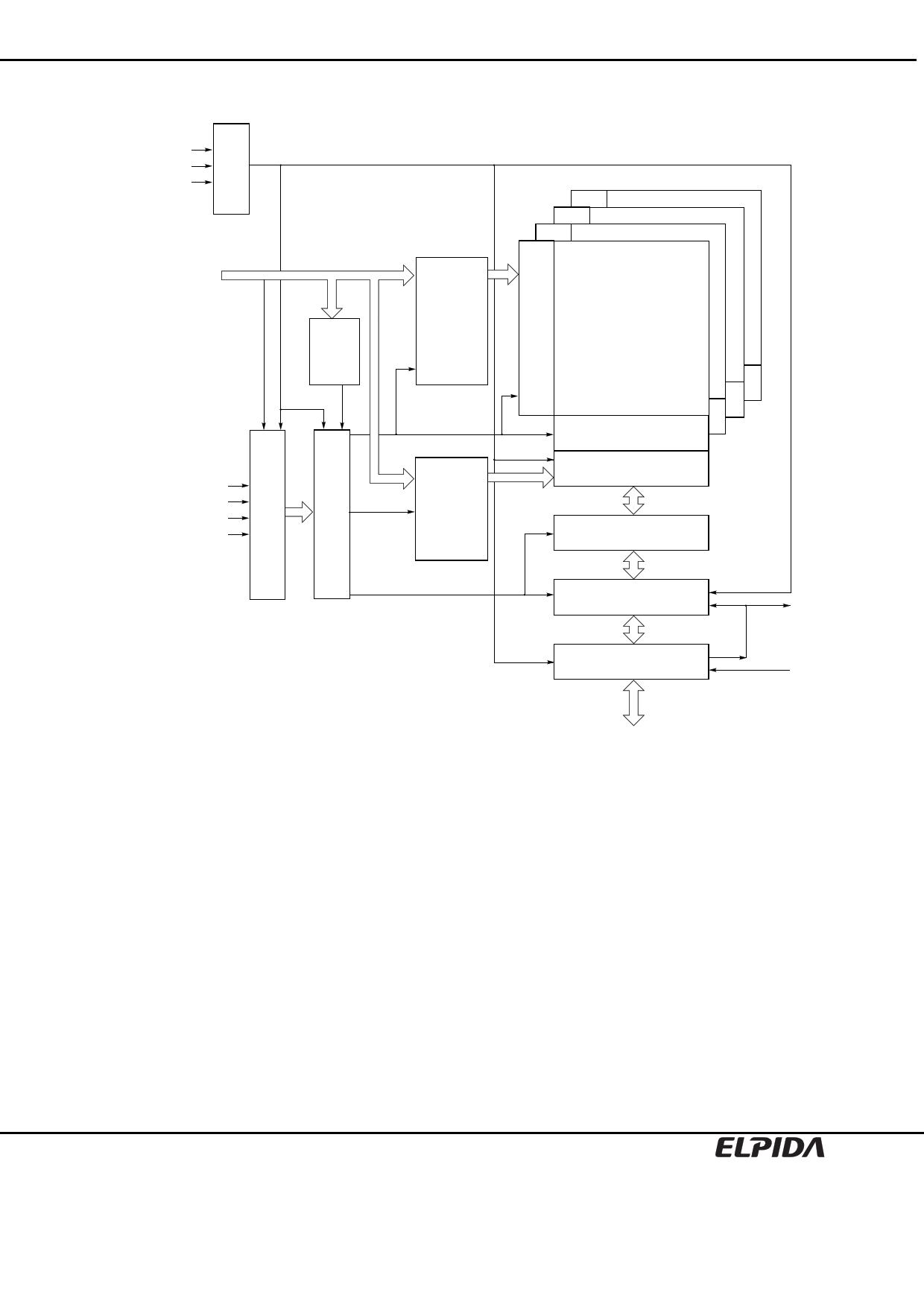
Block Diagram
CK
/CK
CKE
Address, BA0, BA1
Mode
register
Row
address
buffer
and
refresh
counter
/CS
/RAS
/CAS
/WE
Column
address
buffer
and
burst
counter
EDD12322GBH-TS
Bank 3
Bank 2
Bank 1
Memory cell array
Bank 0
Sense amp.
Column decoder
Data control circuit
Latch circuit
Input & Output buffer
DQ
DQS
DM
Preliminary Data Sheet E1530E20 (Ver. 2.0)
11
11 Page | ||
| Páginas | Total 30 Páginas | |
| PDF Descargar | [ Datasheet EDD12322GBH-TS.PDF ] | |
Hoja de datos destacado
| Número de pieza | Descripción | Fabricantes |
| EDD12322GBH-TS | 128M bits DDR Mobile RAM | Elpida Memory |
| Número de pieza | Descripción | Fabricantes |
| SLA6805M | High Voltage 3 phase Motor Driver IC. |
Sanken |
| SDC1742 | 12- and 14-Bit Hybrid Synchro / Resolver-to-Digital Converters. |
Analog Devices |
|
DataSheet.es es una pagina web que funciona como un repositorio de manuales o hoja de datos de muchos de los productos más populares, |
| DataSheet.es | 2020 | Privacy Policy | Contacto | Buscar |
