|
|
|
PDF MCM67M618 Data sheet ( Hoja de datos )
| Número de pieza | MCM67M618 | |
| Descripción | 64K x 18 Bit BurstRAM Synchronous Fast Static RAM | |
| Fabricantes | Motorola Semiconductors | |
| Logotipo | ||
Hay una vista previa y un enlace de descarga de MCM67M618 (archivo pdf) en la parte inferior de esta página. Total 8 Páginas | ||
|
No Preview Available !
MOTOROLA
• SEMICONDUCTOR
TECHNICAL DATA
MCM67M618
Product Preview
64K x 18 Bit BurstRAMTM
Synchronous Fast Static RAM
With Burst Counter and Self-Timed Write
The MCM67M618 is a 1,179,648 bit synchronous static random access memory
designed to provide a burstable, high-performance, secondary cache for the MC68040
and PowerPCTM microprocessors. It is organized as 65,536 words of 18 bits, fabricated
using Motorola's high-performance silicon-gate BiCMOS technology. The device inte-
grates input registers, a 2-bit counter, high speed SRAM, and high drive capability out-
puts onto a single monolithic circuit for reduced parts count implementation of cache
data RAM applications. Synchronous design allows precise cycle control with the use of
an external clock (K). BiCMOS circuitry reduces the overall power consumption of the
integrated functions for greater reliability.
Addresses (AO - A15), data inputs (000 - 0017), and all control signals,
except output enable (G), are clock (K) controlled through positive-edge-
triggered noninverting registers.
Bursts can be initiated with either transfer start processor (TSP) or transfer
start cache controller (TSC) input pins. Subsequent burst addresses are gen-
erated internally by the MCM67M618 (burst sequence imitates that of the
000
DOlO
Vee
Vss
MC68040) and controlled by the burst address advance (BAA) input pin. The
0011
following pages provide more detailed information on burst controls.
Write cycles are internally self-timed and are initiated by the rising edge of
the clock (K) input. This feature eliminates complex off-chip write pulse gen-
eration and provides increased flexibility for incoming signals.
Dual write enables (LW and UW) are provided to allow individually writeable
bytes. LW controls 000 - 008 (the lower bits), while UW controls 009 - 0017
(the upper bits).
This device is ideally suited for systems that require wide data bus widths and
OQ12
OQ13
OQ14
Vss
Vee
OQ15
OQ16
0017
cache memory.
FNPACKAGE
PLASTIC
CASE 778
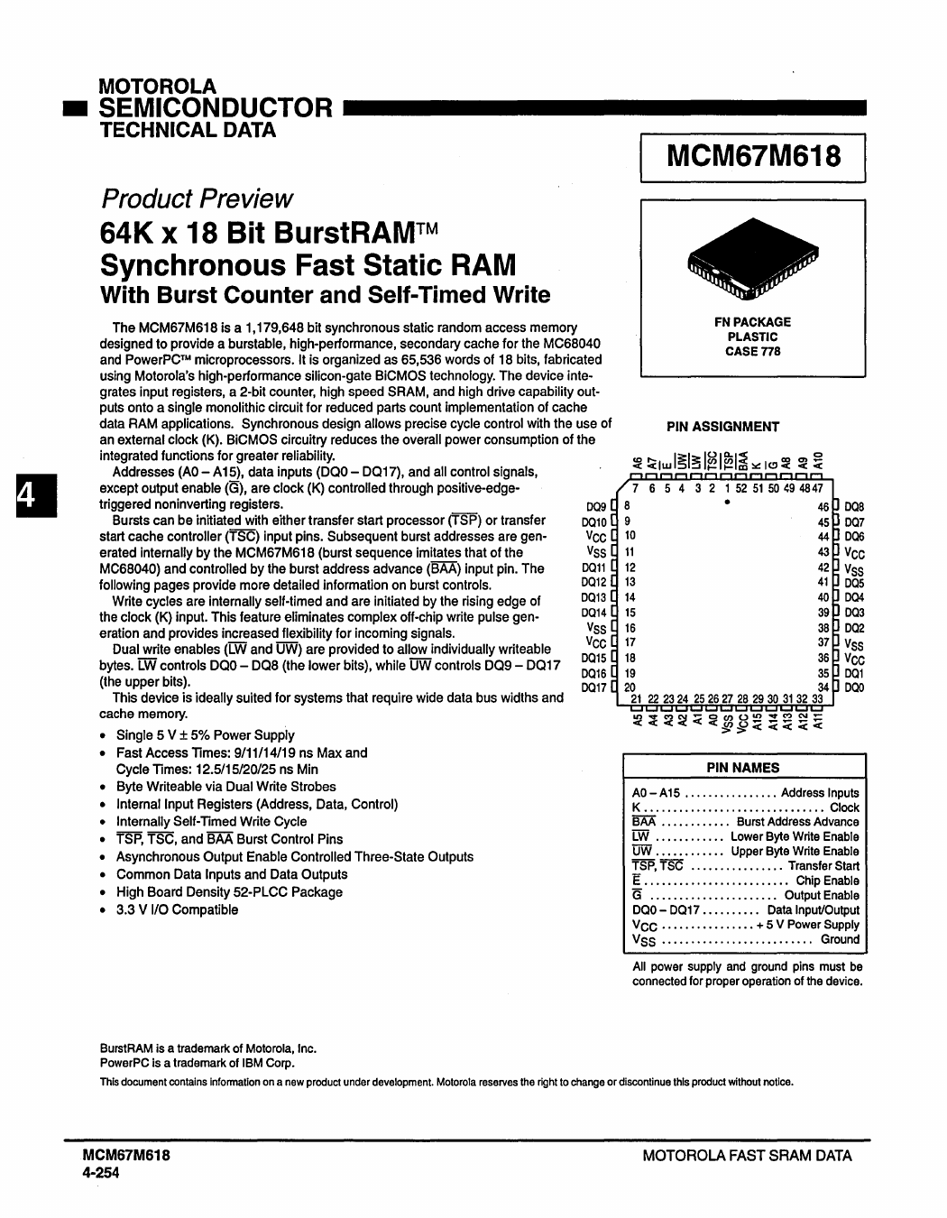
PIN ASSIGNMENT
~ ~lwl~I~I~I~I~~Ic!)~ ~ ~
7 6 5 4 3 2 1 52 51 50 ~9 4847
8 46
9 45
10 44
11 43
12 42
13 41
14 40
15 39
16 38
17 37
18 36
19 35
20 34
21 22 23 24 25 26 27 28 29 30 31 32 33
OQ8
OQ7
000
Vee
VSS
OQ5
0Q4
OQ3
OQ2
Vss
Vee
OQl
OQO
• Single 5 V ± 5% Power Supply
• Fast Access limes: 9/11/14/19 ns Max and
Cycle limes: 12.5/15/20/25 ns Min
• Byte Writeable via Dual Write Strobes
• Internal Input Registers (Address, Data, Control)
• Internally Self-limed Write Cycle
• TSP, TSC, and BAA Burst Control Pins
• Asynchronous Output Enable Controlled Three-State Outputs
• Common Data Inputs and Data Outputs
• High Board Density 52-PLCC Package
• 3.3 V 110 Compatible
PIN NAMES
AO - A15 .••..•.......... Address Inputs
K .....................•........• Clock
BAA ...•.....•.. Burst Address Advance
LW ...••••..... Lower Byte Write Enable
UW • . . . . . . . . . .. Upper Byte Write Enable
TSP, fSC ................ Transfer Start
E . . . . . . . . . . . . . . . . . . . . . . . .. Chip Enable
G ...................... Output Enable
000 - 0017 . . . . . . . . .. Data InpuVOutput
VCC ..•.••.•........ + 5 V Power Supply
VSS .......................... Ground
All power supply and ground pins must be
connected for proper operation of the device.
BurstRAM is a trademark of Motorola, Inc.
PowerPC is a trademark of IBM Corp.
This document contains Information on a new product under development. Motorola reserves the right to change or discontinue this product without notice.
MCM67M618
4-254
MOTOROLA FAST SRAM DATA
1 page 
AC OPERATING CONDITIONS AND CHARACTERISTICS
= =(Vee 5.0 V ± 5% TA 0 to + 70oe, Unless Otherwise Noted)
Input Timing Measurement Reference Level. . . . . . . . . . . . . .. 1.5 V
Input Pulse Levels .. . • • . • . • . . . . • . . . . . . . . . . . . . . . . . .. 0 to 3.0 V
Input Rise/Fall Time .................................... 3 ns
Output Timing Reference Level ........................ " 1.5 V
Output Load ............ See Figure 1A Unless Otherwise Noted
READIWRITE CYCLE TIMING (See Notes 1,2, and 3) (W refers to either or both byte write enables)
Symbol
67M618-9 67M618-11 67M618-14 67M618-19
Parameter
Cycle Time
Clock Access Time
Output Enable to Output Valid
Clock High to Output Active
Clock High to Output Change
Output Enable to Output
Active
Standard Alternate Min Max Min Max Min Max Min Max Unit Notes
tKHKH
tCYC 12.5 -
15 -
20 -
25 -
ns
tKHOV
tco
-
9-
11 - 14 -
19 ns
4
tGLOV tOE - 5 - 5 - 6 - 7 ns
tKHOX1 tOC1
6-
6-
6-
6 - ns
tKHOX2 tOC2
3-
3-
3-
3 - ns
tGLOX
toLZ
0-
0-
0-
0 - ns
Output Disable to 0 High-Z
tGHOZ toHZ 2 6 2 6 2 6 2 7 ns 5
Clock High to 0 High-Z
tKHOZ
tcz
-
6-
6-
6-
6 ns
5
Clock High Pulse Width
tKHKL
tCH
5-
5-
6-
7 - ns
Clock Low Pulse Width
tKLKH
tCL
5-
5-
6-
7 - ns
Setup Times:
Address tAVKH
tAS 2.5 - 2.5 - 2.5 - 3.0 - ns 6
Address Status trSVKH
tss
Data In tOVKH
tos
Write twvKH
tws
Address Advance t8AVKH
Chip Select tEVKH
Hold Times:
Address tKHAX tAH 0.5 - 0.5 - 0.5 - 0.5 - ns 6
Address Status tKHTSX
tSH
Data In tKHOX
tOH
Write tKHWX
twH
Address Advance tKH8AX
Chip Select tKHEX
NOTES:
1. A read cycle is defined by UW and LW high or TSP low for the setup and hold times. A write cycle is defined by LW or UW low and TSP high
for the setup and hold times.
2. All read and write cycle timings are referenced from K or G.
3. G is a don't care when UW or LW is sampled low.
4. Maximum access times are guaranteed for all possible MC68040 external bus cycles.
5. Transition is measured ±500 mV from steady-state voltage with load of Figure 18. This parameter is sampled and not 100% tested. At any
given voltage and temperature, tKHOZ max is less than tKHOX1 min for a given device and from device to device.
6. This is a synchronous device. All addresses must meet the specified setup and hold times for ALL rising edges of clock (K) whenever TSP
or TSC are low and the chip is selected. All other synchronous inputs must meet the specified setup and hold times for ALL rising edges of
Kwhen the chip is selected.Chip enable must be valid at each rising edge of clock for the device (when TSP or TSC is low) to remain enabled.
AC TEST LOADS
:fiOUTPUT!
we
f-= Zo= 50n ::-
L!OUTPUT
255 n
+5V 480n
5pF
(INCLUDING
SCOPE AND JIG)
Figure 1A
Figure 18
NOTE: For information on output I-V characteristics, see Chapter 8, Section 1.
MCM67M618
4·258
MOTOROLA FAST SRAM DATA
5 Page | ||
| Páginas | Total 8 Páginas | |
| PDF Descargar | [ Datasheet MCM67M618.PDF ] | |
Hoja de datos destacado
| Número de pieza | Descripción | Fabricantes |
| MCM67M618 | 64K x 18 Bit BurstRAM Synchronous Fast Static RAM | Motorola Semiconductors |
| MCM67M618A | 64K x 18 Bit BurstRAM Synchronous Fast Static RAM | Motorola Semiconductors |
| MCM67M618B | 64K x 18 Bit BurstRAM Synchronous Fast Static RAM | Motorola Semiconductors |
| Número de pieza | Descripción | Fabricantes |
| SLA6805M | High Voltage 3 phase Motor Driver IC. |
Sanken |
| SDC1742 | 12- and 14-Bit Hybrid Synchro / Resolver-to-Digital Converters. |
Analog Devices |
|
DataSheet.es es una pagina web que funciona como un repositorio de manuales o hoja de datos de muchos de los productos más populares, |
| DataSheet.es | 2020 | Privacy Policy | Contacto | Buscar |