|
|
|
PDF CDP680SG2 Data sheet ( Hoja de datos )
| Número de pieza | CDP680SG2 | |
| Descripción | CMOS High-Performance Silicon-Gate 8-Bit Microcomputer | |
| Fabricantes | GE | |
| Logotipo | ||
Hay una vista previa y un enlace de descarga de CDP680SG2 (archivo pdf) en la parte inferior de esta página. Total 22 Páginas | ||
|
No Preview Available !
_________________ 680S-Series Microprocessors and Microcomputers
Product Preview
CDP680SG2, CDP680SG2C
TERMINAL ASSIGNMENT
mn
TIfO
'eo",
,',".
''""
'''''''s""""""s ""'"""""""0
""""""""""""""""""""
'00
OSCI
om
TIMER
''''''''""""0"""0
'''''"'"""""".
TOP VIEW
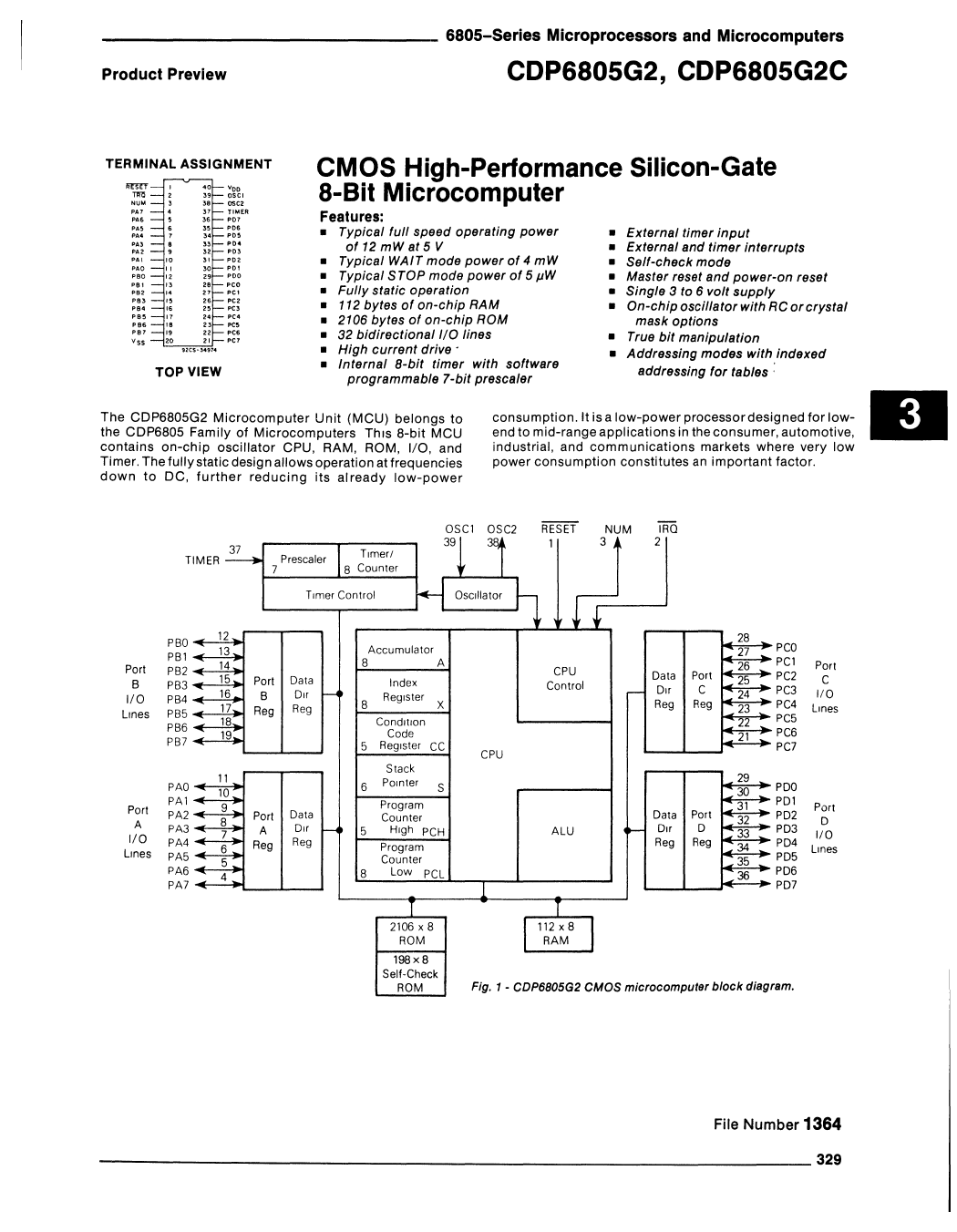
CMOS High-Performance Silicon-Gate
a-Bit Microcomputer
Features:
• Typical full speed operating power
of 12 mWat5 V
• Typical WAIT mode power of 4 mW
• Typical STOP mode power of 5 /JW
• Fully static operation
• 112 bytes of on-chip RAM
• 2106 bytes 01 on-chip ROM
• 32 bidirectionalI/O lines
• High current drive'
• Internal B-bit timer with soltware
programmable 7-bit prescaler
• External timer input
• External and timer interrupts
• Self-check mode
• Master reset and power-on reset
• Single 3 to 6 volt supply
• On-chip oscillator with RC or crystal
mask options
• True bit manipulation
• Addressing modes with indexed
addressing for tables:
The CDP6805G2 Microcomputer Unit (MCU) belongs to
the CDP6805 Family of Microcomputers This 8-bit MCU
contains on-chip oscillator CPU, RAM, ROM, 1/0, and
Timer. The fully static design allows operation at frequencies
down to DC, further reducing its already low-power
consumption. It isa low-powerprocessordesigned for low-
end to mid-range applications in the consumer, automotive,
industrial, and communications markets where very low
power consumption constitutes an important factor.
-=-. .
TIMER
RESET NUM IRO
I3 2
Port
B
1/0
lines
PBO
PBI
PB2
PB3
PB4
PB5
PB6
PB7
Port
A
1/0
Lines
PAO
PAl
PA2
PA3
PA4
PA5
PA6
PA7
Port Data
B D"
Reg Reg
Port
A
Reg
Data
Dir
Reg
Accumulator
8A
Index
Register
8X
Condition
Code
Register CC
Stack
6 POinter
S
Program
Counter
High PCH
Program
Counter
8 low PCl
CPU
CPU
Control
AlU
Data
Dir
Reg
Port
C
Reg
Data
Dir
Reg
Port
D
Reg
PCO
PCI Pon
PC2 C
PC3 1/0
PC4 Lines
PC5
PC6
PC7
PDO
PDI
PD2
PD3
PD4
PD5
PD6
PD7
Port
D
1/0
Lines
198x8
Self· Check
ROM
Fig. 1 - CDP6805G2 CMOS microcomputer block diagram.
File Number 1364
------------___________________________________________________ 329
1 page 
_ _ _ _ _ _ _ _ _ _ _ _ _ _ _ _ 6805-Serles Microprocessors and Microcomputers
CDP6805G2, CDP6805G2C
(;:SE(NS0ITI~VE~~:~*~~W////:0:I W&.:J~ffi
ONLY
~ t LCH
1920 teye
RESET
--------------------------------
~2* ------------------------~
.. INTERNAL TIMING SIGNALS NOT AVAILABLE EXTERNALLY,
* * REPRESENTS THE INTERNAL GATING OF THE CSCI INPUT PIN.
92CS-38101
Fig. 6 - Stop recovery and power-on RESET.
FUNCTIONAL PIN DESCRIPTION
VDD and VSS
Power IS supplied to the MCU uSing these two pins. VDD
IS power and VSS IS ground.
iRO (MASKABLE INTERRUPT REQUEST)
IRQ is mask option selectable With the choice of Interrupt
sensitivity being both level- and negative-edge or negatlve-
edge only.The MCU completes the current Instruction
before It responds to the request. If IRQ IS low and the Inter-
rupt mask bit II bit) In the condition code register IS clear, the
MCU beginS an Interrupt sequence at the end of the current
instruction.
If the mask option IS selected to Include level sensitivity,
then the IRQ Input requires an external resistor to VDD for
"wire-OR" operation. See the Interrupt section for more
detail
RESET
The RESET Input IS not required for start-up but can be
used to reset the MCU's Internal state and provide an orderly
software start-up procedure. Refer to the Reset section for a
detailed deSCription
TIMER
The TIMER Input may be used as an external clock for the
on-chip lImer Refer to Timer section for a detailed deSCrip-
tion.
NUM - NON-USER MODE
This pin IS Intended for use In self-check only User ap-
plications should connect this pin to ground through a 10 kO
resistor
OSC1,OSC2
The CDP6805G2 can be configured to accept either a
crystal input or an RC network. Additionally, the internal
clocks can be derived by either a divide-by-two or divide-
by-four of the external frequency (fOSC). Both of these
options are mask selectable.
RC - If the RC oscillator option IS selected, then a resistor
IS connected to the oscillator pms as shown In Figure 71b)
The relationship between Rand fosc IS shown In Figure 8.
CRYSTAL - The circuit shown In Figure 71a) IS recom-
mended when uSing a crystal. The Internal oscillator IS
deSigned to Interface With an AT-cut parallel resonant quartz
crystal resonator In the frequency range specified for fosc In
the electrical characteristics table. USing an external CMOS
oscillator IS suggested when crystals outside the specified
ranges are to be used. The crystal and components should
be mounted as close as possible to the Input pins to minimize
output distortion and start-up stabilization time Crystal fre-
quency limits are also affected by VDD. Refer to Control
Timing Characteristics for limits. See Table 1
EXTERNAL CLOCK - An external clock should be ap-
plied to the OSC1 Input With the OSC2 Input not connected,
as shown In Figure 71e). An external clock may be used With
either the RC or crystal oscillator mask option. toxOV or
t)LCH do not apply when uSing an external clock input.
III
________________________________________________________________________________ 333
5 Page 
_ _ _ _ _ _ _ _ _ _ _ _ _ _ _ _ 6aOS-Series Microprocessors and Microcomputers
CDP6805G2, CDP6805G2C
machine state dUring Interrupts DUring external or power·
on reset, and dUring a "reset stack pOinter" instruction, the
stack pOinter IS set to Its upper limit ($007F) Nested inter-
rupts and/ or subroutines may use up to 64 (decimal) loca-
tions, beyond which the stack pOinter "wraps around" and
POints to Its upper limit thereby losing the previously stored
Information A subroutine call occupies two RAM bytes on
the stack, while an Int·mupt uses five bytes
CONDITION CODE REGISTER (CC)
The condition code register IS a 5-blt register which in-
dicates the results of the Instruction Just executed These
bits can be indiVidually tested by a program and speCifiC ac-
tion taken as a result of their state Each bit IS explained In
the following paragraphs
HALF CARRY BITS (H) - The H-blt IS set to a one when
a carry occurs between bits 3 and 4 of the ALU dUring an
ADD or ADC instruction The H-blt IS useful In binary coded
decimal subroutines
INTERRUPT MASK BIT (I) - When the I-bit IS set, both
the external Interrupt and the timer Interrupt are disabled
Clearing this bit enables the above Interrupts If an Interrupt
occurs while the I-bit IS set, the Interrupt IS latched and IS
processed when the I-bit IS next cleared.
NEGATIVE (N) - Indicates that the result of the last
arithmetic, logical, or data manipulation IS negative (bit 7 In
the result IS a logical one)
ZERO (Z) - Indicates that the result of the last arithmetic,
logical, or data manipulation IS zero.
CARRY /BORROW (C) - indicates that a carlY or borrow
out of the arithmetic logiC unit (ALU) occurred dUring the
last arithmetic operation This bit IS also affected dUring bit
test and branch instructions, Shifts, and rotates
RESETS
The CDP680SG2 has two reset modes: an active low
external reset pi n (RESET) and a power-on reset function;
refer to Figure S.
RESET
The RESET Input pin IS used to reset the MCU to prOVide
an orderly software start-up procedure When uSing the ex-
ternal reset mode, the RESET pin must stay low tor a mini-
mum of one tcyc The RESET pin IS prOVided with a Schmitt
Trigger Input to Improve ItS nOise Immunity
POWER-ON RESET
The power-on reset occurs when a positive transition IS
detected on VDD. The power-on reset IS used strictly for
power turn-on conditions and should not be used to detect
any drops In the power supply voltage. There IS no provIsion
for a power-down reset The power-on circuitry prOVides for
a 1920 tcyc delay from the time of the first OSCillator opera-
tion If the external RESET Pin IS low at the end of the 1920
tcyc time out, the processor remainS In the reset condition
* Any current instruction including SWI
Either of the two types of reset conditions causes the
following to occur
- Timer control register Interrupt request bit TCR7 IS
cleared to a "0 "
- Timer control register Interrupt mask bit TCR6 IS set to a
"1 "
- All data directIOn register bits are cleared to a "0 " All
ports are defined as Inputs
- Stack pOinter IS set to $G07F
- The Internal address bus IS forced to the reset vector
($1 FFE, $1 FFF)
- Condition code register Interrupt mask bit (I) IS set to a
"1 "
- STOP and WAIT latches are reset
- External Interrupt latch IS reset
All other functions, such as other registers (including out-
put ports), the timer, etc, are not cleared by the reset condi-
tions
INTERRUPTS
The CDP680SG2 may be interrupted by one of three
different methods: either one of two maskable hardware
interrupts (external input or timer) or a nonmaskable
software interrupt (SWI). Systems often require that
normal processing be interrupted so that some external
event may be serviced.
Interrupts cause the processor registers to be saved
on the stack and the interrupt mask (I bit) set to prevent
additional interrupts. The RTI instruction causes the
register contents to be recovered from the stack
followed by a return to normal processing. The stack
order is shown in Figure 13.
Unlike RESET, hardware interrupts do not cause the
current instruction execution to be halted, but are
considered pending until the current instruction
execution is complete.
Note
The current instruction is considered to be the one
already fetched and being operated on.
When the current instruction is complete, the
processor checks all pending hardware interrupts and
if unmasked (I bit clear). proceeds with interrupt
processi ng; otherwise, the next instruction is fetched
and executed. Note that masked interrupts are latched
for later interrupt service.
If both an external interrupt and a timer interrupt are
pending at the end of an instruction execution, the
external Interrupt is serviced first. The SWI is executed
the same as any other instruction and as such takes
precedence over hardware interrupts only if the I bit is
set (hardware interrupts masked). Referto Figure 14 for
the interrupt and instruction processing sequ~
Table 4 shows the execution priority of the RESET,
IRQ and timer interrupts, and instructions (including
the software interrupts, SWI). Two conditions are
shown, one with the I bit set and the other with I bit
clear; however, in either case RESET has the highest
priority of execution. If the I bit is set as per Table 4(a).
the second highest priority is assigned to any instruction
including SWI~is is illustrated in Figure 14 which
shows that the IRQ or Timer interrupts are not executed
when the I bit is set. If the I bit is cleared as per Table
4(b). the priorities change in that the next instruction
.l.§YlI1 or other instruction} is not fetched until after the
IRQ and Timer interrupts have been recognized (and
serviced). Also, when the I bit is clear.JLboth IRQ and
Timer interrupts are pending, the IRQ interrupt is
always serviced before the Timer interrupt.
___________________________________________ 339
11 Page | ||
| Páginas | Total 22 Páginas | |
| PDF Descargar | [ Datasheet CDP680SG2.PDF ] | |
Hoja de datos destacado
| Número de pieza | Descripción | Fabricantes |
| CDP680SG2 | CMOS High-Performance Silicon-Gate 8-Bit Microcomputer | GE |
| CDP680SG2C | CMOS High-Performance Silicon-Gate 8-Bit Microcomputer | GE |
| Número de pieza | Descripción | Fabricantes |
| SLA6805M | High Voltage 3 phase Motor Driver IC. |
Sanken |
| SDC1742 | 12- and 14-Bit Hybrid Synchro / Resolver-to-Digital Converters. |
Analog Devices |
|
DataSheet.es es una pagina web que funciona como un repositorio de manuales o hoja de datos de muchos de los productos más populares, |
| DataSheet.es | 2020 | Privacy Policy | Contacto | Buscar |