|
|
|
PDF CDP6818A Data sheet ( Hoja de datos )
| Número de pieza | CDP6818A | |
| Descripción | CMOS Real-Time Clock | |
| Fabricantes | GE | |
| Logotipo | ||
Hay una vista previa y un enlace de descarga de CDP6818A (archivo pdf) en la parte inferior de esta página. Total 19 Páginas | ||
|
No Preview Available !
__________________________ CMOS Peripherals
Advance Information
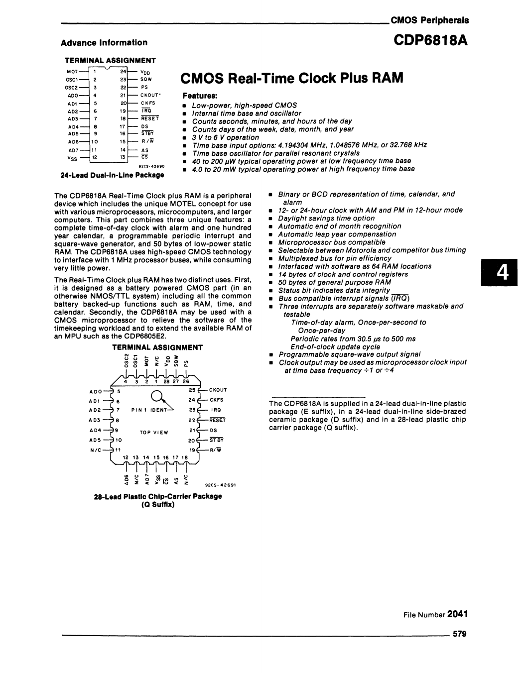
TERMINAL ASSIGNMENT
MOT
OSCI
24 Voo
23 sew
OSC2
ADO
22 PS
21 CKour"
ADI
AD2
AD3
AD4
AD5
7
8
9
20 C KFS
19 TAo
18 'R"E"SE'T
17 os
16 STBY
AD6
10
'5 R/W
"AD7
VSS
'2
cs'4 AS
'3
92C5-42690
24-Lead Dual-In-Llne Package
CDP6818A
CMOS Real-Time Clock Plus RAM
Features:
• Low-power, high-speed CMOS
• Internal time base and oscillator
• Counts seconds, minutes, and hours of the day
• Counts days of the week, date, month, and year
• 3 V to 6 V operation
• Time base input options: 4.194304 MHz, 1.048576 MHz, or 32.768 kHz
• Time base oscillator for parallel resonant crystals
• 40 to 200 pW typical operating power at low frequency time base
• 4.0 to 20 mW typical operating power at high frequency time base
The COP6818A Real-Time Clock plus RAM is a peripheral
device which includes the unique MOTEL concept for use
with various microprocessors, microcomputers, and larger
computers. This part combines three unique features: a
complete time-of-day clock with alarm and one hundred
year calendar, a programmable periodic interrupt and
square-wave generator, and 50 bytes of low-power static
RAM. The COP6818A uses high-speed CMOS technology
to interface with 1 MHz processor buses, while consuming
very little power.
The Real-Time Clock plus RAM has two distinct uses. First,
it is designed as a battery powered CMOS part (in an
otherwise NMOS/TTL system) including all the common
battery backed-up functions such as RAM, time, and
calendar. Secondly, the COP6818A may be used with a
CMOS microprocessor to relieve the software of the
timekeeping workload and to extend the available RAM of
an MPU such as the C0P6805E2.
T£RMINAL ASSIGNMENT
c ;t
>C
o
u>
u>
..
4 3 2 1 28 27 26
PIN'~ADO
AD.
AD2
25 CKOUT
24 CKFS
23 IRQ
AD3
22 RESET
AD4
TOPVIEW
21 OS
AD5
'0
20 ST BY
"N/C
'9
,2 13 14 '5 16 17 18
R/ii
.C
"
z~
...
C
"
!ll~
u>
"
~
Z
92CS-42691
28-Lead Plastic Chip-Carrier Package
(Q Suffix)
• Binary or BCD representation of time, calendar, and
alarm
• 12- or 24-hour clock with AM and PM in 12-hour mode
• Daylight savings time option
• Automatic end of month recognition
• Automatic leap year compensation
• Microprocessor bus compatible
• Selectable between Motorola and competitor bus timing
• Multiplexed bus for pin efficiency
• Interfaced with software as 64 RAM locations
• 14 bytes of clock and control registers
• 50 bytes of general purpose RAM
• Status bit indicates data integrity
• Bus compatible interrupt Signals (IRQ)
• Three interrupts are separately software maskable and
testable
Time-of-day alarm, Once-per-second to
Once-per-day
Periodic rates from 30.5 ps to 500 ms
End-of-clock update cycle
• Programmable square-wave output signal
• Clock output may be used as microprocessor clock input
at time base frequency +1 or +4
lEI
The COP6818A is supplied in a 24-lead dual-in-line plastic
package (E suffix). in a 24-lead dual-in-line side-brazed
ceramic package (0 suffix) and in a 28-lead plastic chip
carrier package (Q suffix).
File Number 2041
------_________________________________________________________ 579
1 page 
_ _ _ _ _ _ _ _ _ _ _ _ _ _ _ _ _ _ _ _ _ _ _ _ _ _ CMOS Peripherals
CDP6818A
ALE (Address Latch Enablel
lAS Pin I
RD IRead Output Enablel
IDS P,nl
WR (Write Enable)
IR/W Pin I
ES (Chip Selectl
ADO·AD7
(Address/ Data 8usl
Fig. 3 - Bus read timing competitor multiplexed bus.
ALE IAddress Latch Enablel
lAS P,nl ------.;;r-
AD IRead Output Enablel
IDS P,nl
WR (Write Enable)
IR/W P,nl
92CS-42694
CS (Chip Selectl
..~---~H--(33)--+--- ...1
-<1ADOAD7
IAddress/Data 8usl ____________
Write Data
Valid
Note VHIGH = VDD - 20 V. VLOW= 08 V. for VDD= 50 V ± 10% for outputs only
VHIGH=20 V. VLOW=O 5 V, for VDD=3 0 V for outputs only
92CS-42695
Fig. 4 - Bus write timing competitor multiplexed bus.
__________________________________________________________ 583
5 Page 
_ _ _ _ _ _ _ _ _ _ _ _ _ _ _ _ _ _ _ _ _ _ _ _ _ _ CMOS Peripherals
CDP6818A
Power-Down Conslderallons
In most systems, the CDP6818A mustcontinueto keep time
when system power is removed. In such systems, a
conversion from system power to an alternate power
supply, usually a battery, must be made. During the
transition from system to battery power, the designer of a
battery backed-up RTC system must protect data integrity,
minimize power consumption, and ensure hardware
reliability.
The stand-by (STBY) pin controls all bus inputs (R/W, DS,
AS, ADO-AD7) STBY, when negated, disallow~r1Y
unintended modification of the RTC data by the bus. STBY
also reduces power consumption by reducing the number
of transitions seen internally.
Power consumption may be further reduced by removing
resistive and capacitive loads from the clock out (CKOUT)
pin and the squarewave (SOW) pin.
During and after the power source conversion, the V'N
maximum specification must never be exceeded. Failure to
meet the V'N maximum specification can cause a virtual
SCR to appear which may result in excessive current drain
and destruction of the part.
Addre.. Map
Figure 14 shows the address map of the CDP6818A. The
memory consists of 50 general purpose RAM bytes, 10 RAM
bytes which normally contain the time, calendar, and alarm
data, and four control and status bytes. All 64 bytes are
directly readable and writable by the processor program
except forthe following: 1) Registers C and D are read only,
2) bit 7 of Register A is read only, and 3) the high-order bit of
the seconds byte is read only. The contents of four control
and status registers (A, B, C, and D) are described in
REGISTERS.
Time, Calendar, and Alarm Locallona
The processor program obtains time and calendar
information by reading the appropriate locations. The
program may initialize the time, calendar, and alarm by
writing to these RAM locations. The contents of the 10 time,
calendar, and alarm bytes may be either binary or binary-
coded decimal (BCD).
Before initializing the internal registers, the SET bit in
Register B should be set to a "1" to prevent time/calendar
updates from occuring. The program initializes the 10
locations in the selected format (binary or BCD), then
indicates the format in the data mode (DM) bitof Register B.
All 10 time, calendar, and alarm bytes must use the same
data mode, either binary or BCD. The SET bit may now be
cleared to allow updates. Once initialized the real-time
clock makes all updates in the selected data mode. The data
mode cannot be changed without reinitializing the 10 data
bytes.
Table 3 shows the binary and BCD formats of the 10 time,
calendar, and alarm locations. The 24/12 bit in Register B
establishes whether the hour locations represent 1-to-12 or
0-to-23. The 24/12 bit cannot be changed without
reinitializing the hour locations. When the 12-hourformat is
selected the high-order bit of the hours byte represent PM
when it is a "1'''.
The time, calendar, and alarm bytes are not always
accessible by the processor program. Once per second the
10 bytes are switched to the update logic to be advanced by
one second and to check for an alarm condition. If any of
the 10 bytes are read at this time, the data outputs are
undefined. The update lockouttime is 2481's at the4.194304
MHz and 1.048567 MHz time bases and 1948 I'S for the
32.768 kHz time base. The Update Cycle section shows how
to accommodate the update cycle in the processor program.
The three alarm bytes may be used in two ways. First, when
the program inserts an alarm time in the appropriate hours,
minutes, and seconds alarm locations, the alarm interrupt is
initiated at the specified time each day if the alarm enable
bit is high. The second usage is to insert a "don'tcare" state
in one or more of three alarm bytes. The "don't care" code is
any hexadecimal byte from CO to FF. That is, the two most-
significant bits of each byte, when set to"1", create a "don't
care" situation. An alarm interrupt each hour is created with
a "don'tcare" code in the hours alarm location. Similarly, an
alarm is generated every minute with "don't care" codes in
the hours and minutes alarm bytes. The "don't care" codes
in all three alarm bytes create an interrupt every second.
,) 00
00
11 DE
50
Bytes
U~8!
RAM
63 3F
0 Seconds
Oil
1 Seconds Alarm
2 Mlnutps
01
02
3 Minutes Alarm
03
4 Hour~
5 Hours Alarm
6 Day of Week
04 8Iil,HY
05 Of BCD
Cotltpntc,
06
7 Date of Month 07
8 MOlllh
08
9 Yt-:ar
09 ,-
10 Register A
11 Register B
OA
DB
12 Register C
OC
13 Register 0
00
Fig. 14 - Address map.
92CS-42705
_____________________________________________ 589
11 Page | ||
| Páginas | Total 19 Páginas | |
| PDF Descargar | [ Datasheet CDP6818A.PDF ] | |
Hoja de datos destacado
| Número de pieza | Descripción | Fabricantes |
| CDP6818 | CMOS Real-Time Clock | GE |
| CDP6818 | CMOS Real Time Clock | Harris Semiconductor |
| CDP6818A | CMOS Real-Time Clock | GE |
| CDP6818A | CMOS Real Time Clock | Harris Semiconductor |
| Número de pieza | Descripción | Fabricantes |
| SLA6805M | High Voltage 3 phase Motor Driver IC. |
Sanken |
| SDC1742 | 12- and 14-Bit Hybrid Synchro / Resolver-to-Digital Converters. |
Analog Devices |
|
DataSheet.es es una pagina web que funciona como un repositorio de manuales o hoja de datos de muchos de los productos más populares, |
| DataSheet.es | 2020 | Privacy Policy | Contacto | Buscar |