|
|
|
PDF ADM1278 Data sheet ( Hoja de datos )
| Número de pieza | ADM1278 | |
| Descripción | Hot Swap Controller and Digital Power and Energy Monitor | |
| Fabricantes | Analog Devices | |
| Logotipo | ||
Hay una vista previa y un enlace de descarga de ADM1278 (archivo pdf) en la parte inferior de esta página. Total 30 Páginas | ||
|
No Preview Available !
Data Sheet
Hot Swap Controller and Digital Power and
Energy Monitor with PMBus Interface
ADM1278
FEATURES
±0.3% accurate, 12-bit ADC for IOUT, VIN, VOUT, and temperature
320 ns response time to short circuit
Shutdown on detection of FET health fault
Constant power foldback for tighter FET SOA protection
Remote temperature sensing with programmable warning
and shutdown thresholds
Resistor-programmable 5 mV to 25 mV VSENSE current limit
Programmable start-up current limit
1% accurate UV, OV, and PWRGD thresholds
Split hot swap and power monitor inputs to allow additional
external ADC filtering
Reports power and energy consumption over time
Peak detect registers for current, voltage, and power
PROCHOT power throttling capability
PMBus fast mode compliant interface
5 mm × 5 mm, 32-lead LFCSP
APPLICATIONS
Servers
Power monitoring and control/power budgeting
Telecommunication and data communication equipment
GENERAL DESCRIPTION
The ADM1278 is a hot swap controller that allows a circuit board
to be removed from or inserted into a live backplane. It also features
current, voltage, power, and temperature readback via an integrated
12-bit analog-to-digital converter (ADC), accessed using a PMBus™
interface. The load current is measured using an internal current
sense amplifier that measures the voltage across a sense resistor
in the power path via the HS+ and HS− pins. A default current
limit of 20 mV is set, but this limit can be adjusted, if required.
The ADM1278 limits the current through the sense resistor by
controlling the gate voltage of an external N-channel FET in the
power path, via the GATE pin. The sense voltage, and therefore
the load current, is maintained below the preset maximum. The
ADM1278 protects the external FET by limiting the time that
the FET remains on while the current is at its maximum value.
This current-limit time is set by the choice of capacitor connected
to the TIMER pin. In addition, a constant power foldback scheme
is used to control the power dissipation in the MOSFET during
power-up and fault conditions. The level of this power, along
with the TIMER regulation time, can be set to ensure that the
MOSFET remains within safe operating area (SOA) limits.
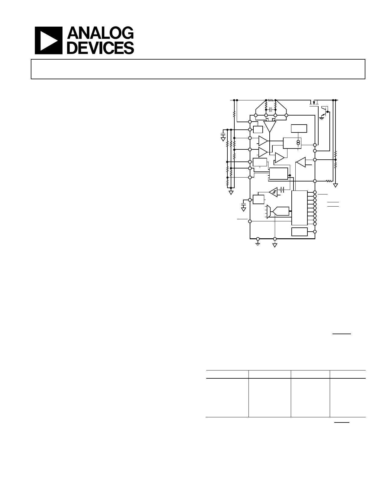
TYPICAL APPLICATION CIRCUIT
4.5V TO 20V
RSENSE
Q1
HS+ MO+
MO– HS–
VCC
VCAP
UV
OV
ISET
PSET
ISTART
LDO
+×50–
ISENSE
ADM1278-1
CHARGE
PUMP
VCP
+
1.0V –
GATE
DRIVE/
LOGIC
–
1.0V +
TIMEOUT
+
REF –
+
SELECT
1.0V
CURRENT-
–
1.0V
HS–
LIMIT
CONTROL
GATE
TEMP
PWGIN
VOUT
VCBOS
TIMER
RETRY
IOUT
TIMER TIMEOUT
HS+
ISENSE
VOUT
TEMP
12-BIT
ADC
LOGIC
AND
PMBus
ANALOG
VOUT
PWRGD
FAULT
ENABLE
GPO2/ALERT2
GPO1/ALERT1/CONV
SCL
SDA
ADR1
ADR2
CSOUT
PGND GND
Figure 1.
In case of a short-circuit event, a fast internal overcurrent
detector responds within 320 ns and signals the gate to shut
down. A 1500 mA pull-down device ensures a fast FET response.
The ADM1278 features overvoltage (OV) and undervoltage (UV)
protection, programmed using external resistor dividers on the
UV and OV pins. A PWRGD signal can be used to detect when
the output supply is valid, using the PWGIN pin to accurately
monitor the output.
The ADM1278 is available in a 32-lead LFCSP with a RETRY pin
that can be configured for automatic retry or latch-off when an
overcurrent fault occurs.
Table 1. Model Options
Model
ADC Accuracy
ADM1278-1AA ±0.3%
ADM1278-1A ±0.7%
ADM1278-1B ±1.0%
ADM1278-2A ±0.7%
ADM1278-3A ±0.7%
SPI Interface
No
No
No
Yes
No
Enable Pin1
Active high
Active high
Active high
Active high
Active low
1 Active high relates to the ENABLE pin, and active low relates to the ENABLE pin.
Rev. A
Document Feedback
Information furnished by Analog Devices is believed to be accurate and reliable. However, no
responsibilityisassumedbyAnalogDevices for itsuse,nor foranyinfringementsofpatentsor other
rights of third parties that may result from its use. Specifications subject to change without notice. No
license is granted by implication or otherwise under any patent or patent rights of Analog Devices.
Trademarksandregisteredtrademarksarethepropertyoftheirrespectiveowners.
One Technology Way, P.O. Box 9106, Norwood, MA 02062-9106, U.S.A.
Tel: 781.329.4700
©2014 Analog Devices, Inc. All rights reserved.
Technical Support
www.analog.com
1 page 
ADM1278
Data Sheet
SPECIFICATIONS
VCC = 4.5 V to 20 V, VCC ≥ VHS+ and VMO+, VHS+ = 2 V to 20 V, VSENSE_HS = (VHS+ − VHS−) = 0 V, TA = −40°C to +85°C, unless otherwise noted.
Table 2.
Parameter1
Symbol
Min Typ Max Unit Test Conditions/Comments
POWER SUPPLY
Operating Voltage Range
Undervoltage Lockout
Undervoltage Hysteresis
Quiescent Current
UV PIN
Input Current
UV Threshold
A Grade and AA Grade
B Grade Only
VCC
UVLO
ICC
IUV
UVTH
4.5 20 V
2.4
2.7 V
VCC rising
90 120 mV
5.5 mA GATE on and power monitor running
50 nA UV ≤ 3.6 V
0.99 1.0 1.01 V
0.97 1.0 1.03 V
UV falling
UV falling
UV Threshold Hysteresis
UV Glitch Filter
UV Propagation Delay
OV PIN
Input Current
OV Threshold
A Grade and AA Grade
B Grade Only
UVHYST
UVGF
UVPD
IOV
OVTH
45 60 75 mV
2 7 μs 50 mV overdrive
58
μs UV low to GATE pull-down active
50 nA OV ≤ 3.6 V
0.99 1.0 1.01 V
0.97 1.0 1.03 V
OV rising
OV rising
OV Threshold Hysteresis
OV Glitch Filter
OV Propagation Delay
HS+ AND HS− PINS
Input Current
Input Imbalance
MO+ AND MO− PINS
Input Current
VCAP PIN
Internally Regulated Voltage
A Grade and AA Grade
B Grade Only
ISET PIN
OVHYST
OVGF
OVPD
ISENSEx
IΔSENSE
IMO±
VVCAP
45 60 75 mV
1.5 3.5 μs 50 mV overdrive
3.0 4.0 μs OV high to GATE pull-down active
150 μA Per individual pin; VHS+, VHS− = 20 V
5 μA IΔSENSE = (I+ − I−)
25 nA Per individual pin; VMO+, VMO− = 20 V
2.68 2.7 2.72 V
2.66 2.7 2.74 V
0 µA ≤ IVCAP ≤ 100 µA; CVCAP = 1 μF
0 µA ≤ IVCAP ≤ 100 µA; CVCAP = 1 μF
Reference Select Threshold
Internal Reference
Gain of Current Sense
Amplifier
Recommended Maximum
Operating Range
Input Current
GATE PIN
GATE Drive Voltage
GATE Pull-Up Current
GATE Pull-Down Current
Regulation
Slow
Fast
GATE Holdoff Resistance
VISETRSTH
VCLREF
AVCSAMP
VISET
IISET
ΔVGATE
IGATEUP
IGATEDN
IGATEDN_REG
IGATEDN_SLOW
IGATEDN_FAST
1.35 1.5 1.65 V
If VISET > VISETRSTH, an internal 1 V reference (VCLREF) is used
1 V Accuracies included in total sense voltage accuracies
50 V/V Accuracies included in total sense voltage accuracies
0.25
1.25 V
5 mV to 25 mV VSENSE current limit
100 nA VISET ≤ VVCAP
Maximum voltage on the gate is always clamped to ≤31 V
ΔVGATE = VGATE − VOUT
10 12 14 V 20 V ≥ VCC ≥ 8 V; IGATE ≤ 5 μA
8 10 V VHS+ = VCC = 5 V; IGATE ≤ 5 μA
7 9 V VHS+ = VCC = 4.5 V; IGATE ≤ 1 μA
−20 −30 μA VGATE = 0 V
45
60 75
μA VGATE ≥ 2 V; VISET = 1.0 V; (VHS+ − VHS−) = 30 mV
5
10 15
mA VGATE ≥ 2 V
750 1500 2250 mA VGATE ≥ 12 V; VCC ≥ 12 V
20 Ω VCC = 0 V, VGATE = 2 V
Rev. A | Page 4 of 61
5 Page 
ADM1278
ABSOLUTE MAXIMUM RATINGS
Table 6.
Parameter
VCC Pin
UV Pin
OV Pin
ISTART Pin
TIMER Pin
TEMP Pin
VCAP Pin
ISET Pin
PSET Pin
FAULT Pin
RETRY Pin
PWGIN Pin
SCL Pin
SDA Pin
SPI_SS Pin
MCLK Pin
MDAT Pin
ADR1 Pin
ADR2 Pin
ENABLE Pin
GPO1/ALERT1/CONV Pin
GPO2/ALERT2 Pin
PWRGD Pin
VOUT Pin
GATE Pin (Internal Supply Only)1
HS+ Pin
HS− Pin
MO+ Pin
MO− Pin
PGND
VSENSE_HS (VHS+ − VHS−)
VSENSE_MO (VMO+ − VMO−)
CSOUT Short-Circuit Duration
Continuous Current into Any Pin
Storage Temperature Range
Operating Temperature Range
Lead Temperature, Soldering (10 sec)
Junction Temperature
Rating
−0.3 V to +25 V
−0.3 V to +4 V
−0.3 V to +4 V
−0.3 V to +4 V
−0.3 V to VCAP + 0.3 V
−0.3 V to VCAP + 0.3 V
−0.3 V to +4 V
−0.3 V to +4 V
−0.3 V to +4 V
−0.3 V to +25 V
−0.3 V to +4 V
−0.3 V to +4 V
−0.3 V to +6.5 V
−0.3 V to +6.5 V
−0.3 V to +4 V
−0.3 V to +4 V
−0.3 V to +4 V
−0.3 V to +6.5 V
−0.3 V to +6.5 V
−0.3 V to +25 V
−0.3 V to +25 V
−0.3 V to +25 V
−0.3 V to +25 V
−0.3 V to +25 V
−0.3 V to +36 V
−0.3 V to +25 V
−0.3 V to +25 V
−0.3 V to +25 V
−0.3 V to +25 V
±0.3 V
±0.3 V
±0.3 V
Indefinite
±10 mA
−65°C to +125°C
−40°C to +85°C
300°C
105°C
1 The GATE pin has internal clamping circuits to prevent the GATE pin voltage
from exceeding the maximum ratings of a MOSFET with gain to source
voltage, VGSMAX = 20 V, and internal process limits. Applying a voltage source
to this pin externally may cause irreversible damage.
Data Sheet
Stresses at or above those listed under Absolute Maximum
Ratings may cause permanent damage to the product. This is a
stress rating only; functional operation of the product at these
or any other conditions above those indicated in the operational
section of this specification is not implied. Operation beyond
the maximum operating conditions for extended periods may
affect product reliability.
THERMAL CHARACTERISTICS
θJA is specified for the worst-case conditions, that is, a device
soldered in a circuit board for surface-mount packages.
Table 7. Thermal Resistance
Package Type
θJA
32-Lead LFCSP (CP-32-13) 32.5
Unit
°C/W
ESD CAUTION
Rev. A | Page 10 of 61
11 Page | ||
| Páginas | Total 30 Páginas | |
| PDF Descargar | [ Datasheet ADM1278.PDF ] | |
Hoja de datos destacado
| Número de pieza | Descripción | Fabricantes |
| ADM1270 | High Voltage Input Protection Device | Analog Devices |
| ADM1272 | High Voltage Positive Hot Swap Controller and Digital Power Monitor | Analog Devices |
| ADM1275 | Hot-Swap Controller and Digital Power Monitor | Analog Devices |
| ADM1276 | Hot Swap Controller and Digital Power and Energy Monitoring | Analog Devices |
| Número de pieza | Descripción | Fabricantes |
| SLA6805M | High Voltage 3 phase Motor Driver IC. |
Sanken |
| SDC1742 | 12- and 14-Bit Hybrid Synchro / Resolver-to-Digital Converters. |
Analog Devices |
|
DataSheet.es es una pagina web que funciona como un repositorio de manuales o hoja de datos de muchos de los productos más populares, |
| DataSheet.es | 2020 | Privacy Policy | Contacto | Buscar |