|
|
|
PDF ADP1190A Data sheet ( Hoja de datos )
| Número de pieza | ADP1190A | |
| Descripción | Integrated 500 mA Load Switch | |
| Fabricantes | Analog Devices | |
| Logotipo | ||
Hay una vista previa y un enlace de descarga de ADP1190A (archivo pdf) en la parte inferior de esta página. Total 13 Páginas | ||
|
No Preview Available !
Data Sheet
FEATURES
Low input voltage range: 1.4 V to 3.6 V
Load switch
Low RDSON_L of 65 mΩ at 3.6 V
500 mA continuous operating current
4 SPST normally open signal switches
RDSON_S of 3 Ω at 1.8 V
Internal charge pump for constant signal switch RDSON
Output discharge resistance (RDIS): 215 Ω at the output side
of the load switch and each analog signal switch output
Built-in level shift for control logic that can operate by
a 1.2 V logic
Ultralow shutdown current: 0.7 µA
Ultrasmall 1.2 mm × 1.6 mm × 0.5 mm, 12-ball,
0.4 mm pitch WLCSP
APPLICATIONS
Mobile phones
SIM card disconnect switches
Digital cameras and audio devices
Portable and battery-powered equipment
GENERAL DESCRIPTION
The ADP1190A is an integrated high-side load switch with four
signal switches designed for operation from 1.4 V to 3.6 V. This
load switch provides power domain isolation for extended power
battery life. The load switch is a low on-resistance P-channel
MOSFET that supports up to 500 mA of continuous load
current and minimizes power loss. Integrated with the load
switch are four normally open, 3 Ω single pole, single throw
(SPST) signal switches controlled by the charge pump.
Integrated 500 mA Load Switch
with Quad Signal Switch
ADP1190A
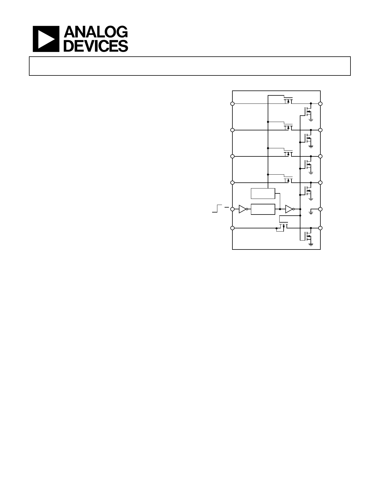
FUNCTIONAL BLOCK DIAGRAM
S1 T1
S2 T2
S3 T3
S4
OFF
EN
ON
CHARGE
PUMP
5ms
DEBOUNCE
IN
ADP1190A
LOAD
SWITCH
Figure 1.
T4
GND
OUT
Beyond its excellent operating performance, the ADP1190A
occupies minimal printed circuit board (PCB) space with an
area less than 1.92 mm2 and a height of 0.50 mm. The ADP1190A
is available in an ultrasmall 1.2 mm × 1.6 mm × 0.5 mm, 12-ball,
0.4 mm pitch WLCSP.
Rev. 0
Document Feedback
Information furnished by Analog Devices is believed to be accurate and reliable. However, no
responsibilityisassumedbyAnalogDevices for itsuse,nor foranyinfringementsofpatentsor other
rights of third parties that may result from its use. Specifications subject to change without notice. No
license is granted by implication or otherwise under any patent or patent rights of Analog Devices.
Trademarksandregisteredtrademarksarethepropertyoftheirrespectiveowners.
One Technology Way, P.O. Box 9106, Norwood, MA 02062-9106, U.S.A.
Tel: 781.329.4700
©2013 Analog Devices, Inc. All rights reserved.
Technical Support
www.analog.com
1 page 
ADP1190A
ABSOLUTE MAXIMUM RATINGS
Table 2.
Parameter
VIN to GND
VOUT to GND
Sx to GND
Tx to GND
EN to GND
Continuous Load Switch Current
TA = 25°C
TA = 85°C
Continuous Diode Current
Storage Temperature Range
Junction Temperature
Operating Temperature Range
Junction Temperature Range
Ambient Temperature Range
Soldering Conditions
Rating
−0.3 V to +4.0 V
−0.3 V to VIN
−0.3 V to +4.0 V
−0.3 V to +4.0 V
−0.3 V to +4.0 V
±1 A
±500 mA
−50 mA
−65°C to +150°C
150°C
−40°C to +125°C
−40°C to +85°C
JEDEC J-STD-020
Stresses above those listed under Absolute Maximum Ratings
may cause permanent damage to the device. This is a stress
rating only; functional operation of the device at these or any
other conditions above those indicated in the operational
section of this specification is not implied. Exposure to absolute
maximum rating conditions for extended periods may affect
device reliability.
THERMAL DATA
Absolute maximum ratings apply individually only, not in
combination. The ADP1190A can be damaged when the
junction temperature limits are exceeded. Monitoring ambient
temperature does not guarantee that the junction temperature (TJ)
is within the specified temperature limits. In applications with
high power dissipation and poor thermal resistance, the
maximum ambient temperature may need to be derated.
In applications with moderate power dissipation and low PCB
thermal resistance, the maximum ambient temperature can
exceed the maximum limit as long as the junction temperature
is within specification limits. The TJ of the device is dependent
on the ambient temperature (TA), the power dissipation of the
device (PD), and the junction-to-ambient thermal resistance of
the package (θJA).
Maximum TJ is calculated from TA and PD using the formula
TJ = TA + (PD × θJA)
Data Sheet
The junction-to-ambient thermal resistance (θJA) of the package
is based on modeling and calculation using a 4-layer board. The
junction-to-ambient thermal resistance is highly dependent on
the application and board layout. In applications where high
maximum power dissipation exists, close attention to thermal
board design is required. The value of θJA can vary, depending
on PCB material, layout, and environmental conditions. The
specified value of θJA is based on a 4-layer, 4 inch × 3 inch circuit
board. See JESD51-7 and JESD51-9 for detailed information
on the board construction. For additional information, see the
AN-617 Application Note, Wafer Level Chip Scale Package.
ΨJB is the junction-to-board thermal characterization parameter
with units of °C/W. ΨJB of the package is based on modeling and
calculation using a 4-layer board. JESD51-12, Guidelines for
Reporting and Using Electronic Package Thermal Information,
states that thermal characterization parameters are not the same
as thermal resistances. ΨJB measures the component power
flowing through multiple thermal paths rather than through a
single path as in thermal resistance (θJB). Therefore, ΨJB thermal
paths include convection from the top of the package as well as
radiation from the package, factors that make ΨJB more useful
in real-world applications. Maximum TJ is calculated from the
board temperature (TB) and PD using the formula
TJ = TB + (PD × ΨJB)
See JESD51-8 and JESD51-12 for more detailed information
about ΨJB.
THERMAL RESISTANCE
θJA and ΨJB are specified for the worst-case conditions, that is, a
device soldered in a circuit board for surface-mount packages.
Table 3. Thermal Resistance
Package Type
θJA ΨJB
Unit
12-Ball WLCSP
130 29.2 °C/W
ESD CAUTION
Rev. 0 | Page 4 of 12
5 Page 
ADP1190A
MICROCONTROLLER
S1
S2
S3
VIN = 1.4V TO 3.6V
S4
CHARGE
PUMP
EN 5ms
DEBOUNCE
IN
ADP1190A
LOAD
SWITCH
Data Sheet
CONNECTOR
SIM CARD
T1
I/O
T2
I/O
T3
RST
T4
CLK
GND
OUT
GND
VCC
Figure 22. Typical Application Diagram
50Ω
Sx
VS
VOUT
Tx
50Ω
NETWORK
ANALYZER
Figure 23. Bandwidth Measurement Setup
Rev. 0 | Page 10 of 12
11 Page | ||
| Páginas | Total 13 Páginas | |
| PDF Descargar | [ Datasheet ADP1190A.PDF ] | |
Hoja de datos destacado
| Número de pieza | Descripción | Fabricantes |
| ADP1190 | Integrated 500 mA Load Switch | Analog Devices |
| ADP1190A | Integrated 500 mA Load Switch | Analog Devices |
| Número de pieza | Descripción | Fabricantes |
| SLA6805M | High Voltage 3 phase Motor Driver IC. |
Sanken |
| SDC1742 | 12- and 14-Bit Hybrid Synchro / Resolver-to-Digital Converters. |
Analog Devices |
|
DataSheet.es es una pagina web que funciona como un repositorio de manuales o hoja de datos de muchos de los productos más populares, |
| DataSheet.es | 2020 | Privacy Policy | Contacto | Buscar |