|
|
|
PDF HMC7587 Data sheet ( Hoja de datos )
| Número de pieza | HMC7587 | |
| Descripción | 81 GHz to 86 GHz E-Band I/Q Downconverter | |
| Fabricantes | Analog Devices | |
| Logotipo | ||
Hay una vista previa y un enlace de descarga de HMC7587 (archivo pdf) en la parte inferior de esta página. Total 30 Páginas | ||
|
No Preview Available !
Data Sheet
FEATURES
Conversion gain: 10 dB typical
Image rejection: 30 dBc typical
Noise figure: 6 dB typical
Input power for 1 dB compression (P1dB): −10 dBm typical
Input third-order intercept (IP3): −2 dBm typical
Input second-order intercept (IP2): 25 dBm typical
6× LO leakage at RFIN: −40 dBm typical
Radio frequency (RF) return loss: 10 dB typical
Local oscillator (LO) return loss: 20 dB typical
Die size: 3.599 mm × 2.199 mm × 0.05 mm
APPLICATIONS
E-band communication systems
High capacity wireless backhauls
Test and measurement
81 GHz to 86 GHz
E-Band I/Q Downconverter
HMC7587
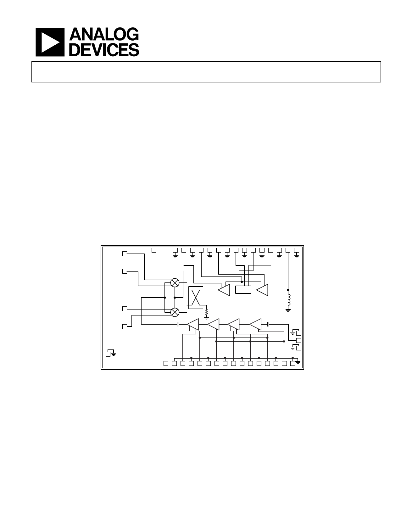
GENERAL DESCRIPTION
The HMC7587 is an integrated, E-band gallium arsenide (GaAs),
monolithic microwave integrated circuit (MMIC), in-phase/
quadrature (I/Q) downconverter chip that operates from 81 GHz
to 86 GHz. The HMC7587 provides a small signal conversion
gain of 10 dB with 30 dBc of image rejection across the frequency
band. The device uses a low noise amplifier followed by an image
rejection mixer that is driven by a 6× multiplier.
The image rejection mixer eliminates the need for a filter following
the low noise amplifier. Differential I and Q mixer outputs are
provided for direct conversion applications. Alternatively, the
outputs can be combined using an external 90° hybrid and two
external 180° hybrids to allow for single-sideband applications. All
data includes the effect of a 3 mil wide ribbon wedge bond on the
RF port, and a 1 mil gold wire wedge bond on the intermediate
frequency (IF) ports.
IFIP 5
IFIN 4
FUNCTIONAL BLOCK DIAGRAM
6 7 8 9 10 11 12 13 14 15 16 17 18 19 20 21
×6
IFQN 3
IFQP 2
HMC7587
1
RFIN
22
23
24
40 39 38 37 36 35 34 33 32 31 30 29 28 27 26 25
Figure 1.
Rev. A
Document Feedback
Information furnished by Analog Devices is believed to be accurate and reliable. However, no
responsibility is assumed by Analog Devices for its use, nor for any infringements of patents or other
rights of third parties that may result from its use. Specifications subject to change without notice. No
license is granted by implication or otherwise under any patent or patent rights of Analog Devices.
Trademarksandregisteredtrademarksarethepropertyoftheirrespectiveowners.
One Technology Way, P.O. Box 9106, Norwood, MA 02062-9106, U.S.A.
Tel: 781.329.4700
©2016 Analog Devices, Inc. All rights reserved.
Technical Support
www.analog.com
1 page 
HMC7587
ABSOLUTE MAXIMUM RATINGS
Table 2.
Parameter
Drain Bias Voltage
VDAMP1, VDAMP2
VDMULT
VDLNA1, VDLNA2, VDLNA3, VDLNA4
Gate Bias Voltage
VGAMP
VGX2, VGX3
VGLNA1, VGLNA2, VGLNA3, VGLNA4
VGMIX
LO Input Power
Maximum Junction Temperature (to
Maintain 1 Million Hours Mean Time to
Failure (MTTF))
Storage Temperature Range
Operating Temperature Range
Rating
4.5 V
3V
4.5 V
−3 V to 0 V
−3 V to 0 V
−3 V to 0 V
−3 V to 0 V
10 dBm
175°C
−65°C to +150°C
−55°C to +85°C
Stresses at or above those listed under Absolute Maximum
Ratings may cause permanent damage to the product. This is a
stress rating only; functional operation of the product at these
or any other conditions above those indicated in the operational
section of this specification is not implied. Operation beyond
the maximum operating conditions for extended periods may
affect product reliability.
Data Sheet
THERMAL RESISTANCE
Table 3. Thermal Resistance
Package Type
40-Pad Bare Die [CHIP]
θJC1
61.7
Unit
°C/W
1 Based on ABLEBOND® 84-1LMIT as die attach epoxy with thermal
conductivity of 3.6 W/mK.
ESD CAUTION
Rev. A | Page 4 of 55
5 Page 
HMC7587
50
45
40 TA = +85°C
TA = +25°C
35 TA = –55°C
30
25
20
15
10
5
0
81.0 81.5 82.0 82.5 83.0 83.5 84.0 84.5 85.0 85.5 86.0
RF FREQUENCY (GHz)
Figure 27. Input IP2 vs. RF Frequency at Various Temperatures,
RFIN = −20 dBm, LO = 2 dBm, IF = 500 MHz, VDLNA = 4 V
50
45 LO = –4dBm
LO = –2dBm
40 LO = 0dBm
LO = +2dBm
35 LO = +4dBm
LO = +6dBm
30 LO = +8dBm
25
20
15
10
5
0
81.0 81.5 82.0 82.5 83.0 83.5 84.0 84.5 85.0 85.5 86.0
RF FREQUENCY (GHz)
Figure 28. Input IP2 vs. RF Frequency at Various LO Powers,
RFIN = −20 dBm, IF = 500 MHz, VDLNA = 4 V
50
45
40
35
30
25
20
15
IDLNA = 5mA
IDLNA = 30mA
IDLNA = 10mA
IDLNA = 35mA
10
IDLNA = 15mA
IDLNA = 40mA
IDLNA = 20mA
IDLNA = 45mA
5
IDLNA = 25mA
IDLNA = 50mA
0
81.0 81.5 82.0 82.5 83.0 83.5 84.0 84.5 85.0 85.5 86.0
RF FREQUENCY (GHz)
Figure 29. Input IP2 vs. RF Frequency at Various IDLNA Values,
RFIN = −20 dBm, LO = 2 dBm, IF = 500 MHz, VDLNA = 4 V
Data Sheet
50
45
40 TA = +85°C
TA = +25°C
35 TA = –55°C
30
25
20
15
10
5
0
81.0 81.5 82.0 82.5 83.0 83.5 84.0 84.5 85.0 85.5 86.0
RF FREQUENCY (GHz)
Figure 30. Input IP2 vs. RF Frequency at Various Temperatures,
RFIN = −20 dBm, LO = 2 dBm, IF = 500 MHz, VDLNA = 3 V
50
45 LO = –4dBm
LO = –2dBm
40 LO = 0dBm
LO = +2dBm
35 LO = +4dBm
LO = +6dBm
30 LO = +8dBm
25
20
15
10
5
0
81.0 81.5 82.0 82.5 83.0 83.5 84.0 84.5 85.0 85.5 86.0
RF FREQUENCY (GHz)
Figure 31. Input IP2 vs. RF Frequency at Various LO Powers,
RFIN = −20 dBm, IF = 500 MHz, VDLNA = 3 V
50
45
40
35
30
25
20
15
IDLNA = 5mA
IDLNA = 30mA
IDLNA = 10mA
IDLNA = 35mA
10
IDLNA = 15mA
IDLNA = 40mA
IDLNA = 20mA
IDLNA = 45mA
5
IDLNA = 25mA
IDLNA = 50mA
0
81.0 81.5 82.0 82.5 83.0 83.5 84.0 84.5 85.0 85.5 86.0
RF FREQUENCY (GHz)
Figure 32. Input IP2 vs. RF Frequency at Various IDLNA Values,
RFIN = −20 dBm, LO = 2 dBm, IF = 500 MHz, VDLNA = 3 V
Rev. A | Page 10 of 55
11 Page | ||
| Páginas | Total 30 Páginas | |
| PDF Descargar | [ Datasheet HMC7587.PDF ] | |
Hoja de datos destacado
| Número de pieza | Descripción | Fabricantes |
| HMC7586 | E-Band I/Q Downconverter | Analog Devices |
| HMC7587 | 81 GHz to 86 GHz E-Band I/Q Downconverter | Analog Devices |
| HMC758LP3 | GaAs SMT PHEMT LOW NOISE AMPLIFIER | Hittite Microwave Corporation |
| HMC758LP3E | GaAs SMT PHEMT LOW NOISE AMPLIFIER | Hittite Microwave Corporation |
| Número de pieza | Descripción | Fabricantes |
| SLA6805M | High Voltage 3 phase Motor Driver IC. |
Sanken |
| SDC1742 | 12- and 14-Bit Hybrid Synchro / Resolver-to-Digital Converters. |
Analog Devices |
|
DataSheet.es es una pagina web que funciona como un repositorio de manuales o hoja de datos de muchos de los productos más populares, |
| DataSheet.es | 2020 | Privacy Policy | Contacto | Buscar |