|
|
|
PDF HMC625BLP5E Data sheet ( Hoja de datos )
| Número de pieza | HMC625BLP5E | |
| Descripción | 0.5 dB LSB GaAs MMIC 6-BIT DIGITAL VARIABLE GAIN AMPLIFIER | |
| Fabricantes | Analog Devices | |
| Logotipo | ||
Hay una vista previa y un enlace de descarga de HMC625BLP5E (archivo pdf) en la parte inferior de esta página. Total 10 Páginas | ||
|
No Preview Available !
Typical Applications
The HMC625BLP5E is ideal for:
• Cellular/3G Infrastructure
• WiBro / WiMAX / 4G
• Microwave Radio & VSAT
• Test Equipment and Sensors
• IF & RF Applications
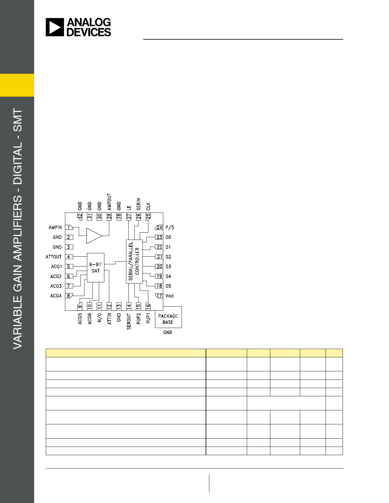
Functional Diagram
HMC625BLP5E
v02.0616
0.5 dB LSB GaAs MMIC 6-BIT DIGITAL
VARIABLE GAIN AMPLIFIER, DC - 5 GHz
Features
-13.5 to +18 Gain Control in 0.5 dB Steps
Power-up State Selection
High Output IP3: +32 dBm
TTL/CMOS Compatible
Serial, Parallel, or latched Parallel Control
±0.25 dB Typical Gain Step Error
Single +5V Supply
32 Lead 5x5 mm SMT Package: 25 mm2
General Description
The HMC625BLP5E is a digitally controlled variable
gain amplifier which operates from DC to 5 GHz, and
can be programmed to provide anywhere from 13.5
dB attenuation, to 18 dB of gain, in 0.5 dB steps. The
HMC625BLP5E delivers noise figure of 6 dB in its
maximum gain state, with output IP3 of up to +32 dBm
in any state. The dual mode control interface is CMOS/
TTL compatible, and accepts either a three wire serial
input or a 6 bit parallel word. The HMC625BLP5E also
features a user selectable power up state and a serial
output port for cascading other Hittite serial controlled
components. The HMC625BLP5E is housed in a
RoHS compliant 5x5 mm QFN leadless package, and
requires no external matching components.
Electrical Specifications, TA = +25° C, 50 Ohm System, Vdd= +5V, Vs= +5V
Parameter
Frequency
Min.
Typ.
Max.
Gain (Maximum Gain State)
DC - 3.0 GHz
3.0 - 5.0 GHz
13
5
18
13
Gain Control Range
31.5
Input Return Loss
DC - 5.0 GHz
15
Output Return Loss
DC - 5.0 GHz
10
Gain Accuracy: (Referenced to Maximum Gain State)
All Gain States
DC - 0.8 GHz
0.8 - 5.0 GHz
± (0.10 + 5% of Gain Setting) Max.
± (0.30 + 3% of Gain Setting) Max.
Output Power for 1dB Compression
DC - 3.0 GHz
3.0 - 5.0 GHz
16
13
19
16
Output Third Order Intercept Point
(Two-Tone Output Power= 0 dBm Each Tone, 1 MHz Spacing)
DC - 5.0 GHz
32
Noise Figure
900 MHz
6
Total Supply Current (Idd + Is)
DC - 5.0 GHz
60
87.5
100
Units
dB
dB
dB
dB
dB
dB
dB
dBm
dBm
dBm
dB
mA
Information furnished by Analog Devices is believed to be accurate and reliable. However, no For price, delivery, and to place orders: Analog Devices, Inc.,
1 responsibility is assumed by Analog Devices for its use, nor for any infringements of patents or other
rights of third parties that may result from its use. Specifications subject to change without notice. No
license is granted by implication or otherwise under any patent or patent rights of Analog Devices.
Trademarks and registered trademarks are the property of their respective owners.
One Technology Way, P.O. Box 9106, Norwood, MA 02062-9106
Phone: 781-329-4700 • Order online at www.analog.com
Application Support: Phone: 1-800-ANALOG-D
1 page 
HMC625BLP5E
v02.0616
0.5 dB LSB GaAs MMIC 6-BIT DIGITAL
VARIABLE GAIN AMPLIFIER, DC - 5 GHz
Serial Control Interface
The HMC625BLP5E contains a 3-wire SPI compatible digital interface (SERIN, CLK, LE). It is activated when P/S
is kept high. The 6-bit serial word must be loaded MSB first. The positive-edge sensitive CLK and LE requires
clean transitions. If mechanical switches were used, sufficient debouncing should be provided. When LE is high,
6-bit data in the serial input register is transferred to the attenuator. When LE is high CLK is masked to prevent data
transition during output loading.
When P/S is low, 3-wire SPI interface inputs (SERIN, CLK, LE) are disabled and serial input register is loaded
asynchronously with parallel digital inputs (D0-D5). When LE is high, 6-bit parallel data is transferred to the attenuator.
For all modes of operations, the DVGA state will stay constant while LE is kept low.
Parameter
Min. serial period, tSCK
Control set-up time, tCS
Control hold-time, tCH
LE setup-time, tLN
Min. LE pulse width, tLEW
Min LE pulse spacing, tLES
Serial clock hold-time from LE, tCKN
Hold Time tPH
Latch Enable Minimum width, tLEN
Setup Time, tPS
Typ.
100 ns
20 ns
20 ns
10 ns
10 ns
630 ns
10 ns
0 ns
10 ns
2 ns
Timing Diagram (Latched Parallel Mode)
Parallel Mode (Direct Parallel Mode & Latched Parallel Mode)
Note: The parallel mode is enabled when P/S is set to low.
Direct Parallel Mode - The attenuation state is changed by the Control Voltage Inputs directly. The LE (Latch Enable)
must be at a logic high to control the attenuator in this manner.
Latched Parallel Mode - The attenuation state is selected using the Control Voltage Inputs and set while the LE is in
the Low state. The attenuator will not change state while LE is Low. Once all Control Voltage Inputs are at the desired
states the LE is pulsed. See timing diagram above for reference.
For price, delivery, and to place orders: Analog Devices, Inc., One Technology Way, P.O. Box 9106, Norwood, MA 02062-9106
Phone: 781-329-4700 • Order online at www.analog.com
Application Support: Phone: 1-800-ANALOG-D
4
5 Page | ||
| Páginas | Total 10 Páginas | |
| PDF Descargar | [ Datasheet HMC625BLP5E.PDF ] | |
Hoja de datos destacado
| Número de pieza | Descripción | Fabricantes |
| HMC625BLP5E | 0.5 dB LSB GaAs MMIC 6-BIT DIGITAL VARIABLE GAIN AMPLIFIER | Analog Devices |
| Número de pieza | Descripción | Fabricantes |
| SLA6805M | High Voltage 3 phase Motor Driver IC. |
Sanken |
| SDC1742 | 12- and 14-Bit Hybrid Synchro / Resolver-to-Digital Converters. |
Analog Devices |
|
DataSheet.es es una pagina web que funciona como un repositorio de manuales o hoja de datos de muchos de los productos más populares, |
| DataSheet.es | 2020 | Privacy Policy | Contacto | Buscar |