|
|
|
PDF MT18HVF12872 Data sheet ( Hoja de datos )
| Número de pieza | MT18HVF12872 | |
| Descripción | 1GB DDR2 VLP Registered DIMM | |
| Fabricantes | Micron | |
| Logotipo | ||
Hay una vista previa y un enlace de descarga de MT18HVF12872 (archivo pdf) en la parte inferior de esta página. Total 15 Páginas | ||
|
No Preview Available !
1GB (x72, ECC, SR) 240-Pin DDR2 VLP RDIMM
Features
DDR2 VLP Registered DIMM (RDIMM)
MT18HVF12872(P) – 1GB
For the latest data sheet and for component data sheets, refer to Micron's Web site: www.micron.com/products/ddr2
Features
• Supports 95°C with double refresh
• Fits with the ATCA form factor
• 240-pin, registered dual in-line memory module
• Fast data transfer rates: PC2-3200, PC2-4200, or PC2-5300
• Supports ECC error detection and correction
• VDD = VDDQ = +1.8V
• VDDSPD = +1.7V to +3.6V
• JEDEC-standard 1.8V I/O (SSTL_18-compatible)
• Differential data strobe (DQS, DQS#) option
• 4-bit prefetch architecture
• DLL to align DQ and DQS transitions with CK
• Single rank
• Multiple internal device banks for concurrent
operation
• Programmable CAS# latency (CL)
• Posted CAS# additive latency (AL)
• WRITE latency = READ latency - 1 tCK
• Programmable burst lengths: 4 or 8
• Adjustable data-output drive strength
• 64ms, 8,192-cycle refresh
• On-die termination (ODT)
• Serial presence-detect (SPD) with EEPROM
• Gold edge contacts
Table 1: Addressing
Refresh count
Row address
Device bank address
Device page size per bank
Device configuration
Column address
Module rank address
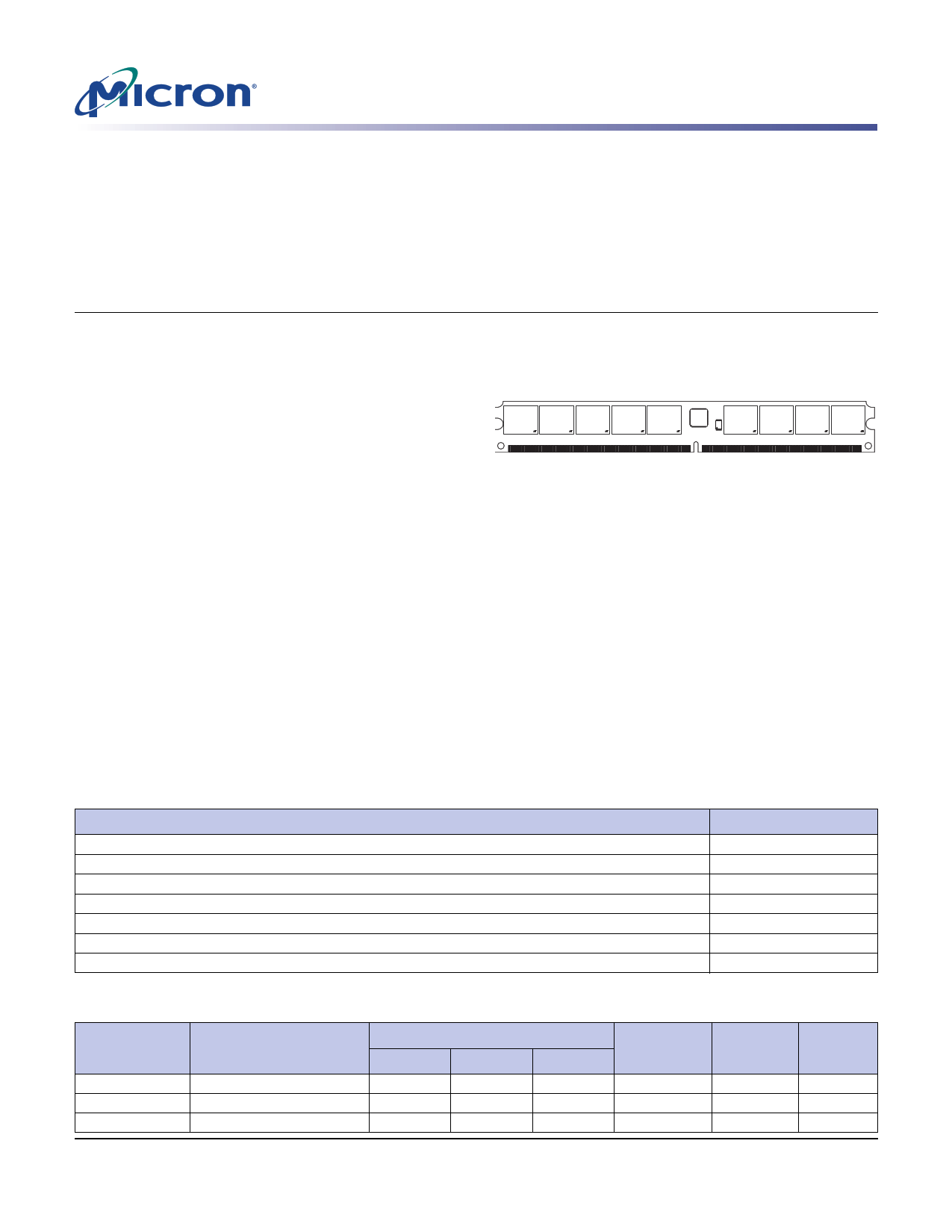
Figure 1:
240-Pin VLP DIMM (MO-237)
Functionally equivelent to R/C “U” and “V”
Height: 17.9mm (0.705in)
Options
Marking
• Parity
• Package
240-pin DIMM (lead-free)
• Frequency/CAS latency1
3.0ns @ CL = 5 (DDR2-667)2
3.75ns @ CL = 4 (DDR2-533)
5.0ns @ CL = 3 (DDR2-400)
• PCB height
17.9mm (1.18in)
P
Y
-667
-53E
-40E
Notes: 1. CL = CAS (READ) latency; registered mode
will add one clock cycle to CL.
2. Contact Micron for product availability.
1GB
8K
16K (A0–A13)
4 (BA0, BA1)
1KB
512Mb (128 Meg x 4)
2K (A0–A9, A11)
1 (S0#)
Table 2: Key Timing Parameters
Speed Grade
-667
-53E
-40E
Industry Nomenclature
PC2-5300
PC2-4200
PC2-3200
Data Rate (MT/s)
CL = 5
667
–
–
CL = 4
533
533
400
CL = 3
–
400
400
tRCD
(ns)
15
15
15
tRP
(ns)
15
15
15
tRC
(ns)
55
55
55
PDF: 09005aef82255aba/Source: 09005aef82255a83
HVF18C64_128_256x72G.fm - Rev. B 5/06 EN
1 Micron Technology, Inc., reserves the right to change products or specifications without notice.
©2003 Micron Technology, Inc. All rights reserved.
Products and specifications discussed herein are subject to change by Micron without notice.
1 page 
1GB (x72, ECC, SR) 240-Pin DDR2 VLP RDIMM
Pin Assignments and Descriptions
Table 5:
Pin Descriptions (continued)
Refer to Table 4 on page 3 for more information
Symbol
VREF
VSS
VDDSPD
NC
RFU
Type
Supply
Supply
Supply
–
–
Source
DRAM,
PLL,
Register
ALL
SPD
SSTL_18 reference voltage.
Description
Ground.
Serial EEPROM positive power supply: +1.7V to +3.6V.
No connect: These pins should be left unconnected.
Reserved for future use.
PDF: 09005aef82255aba/Source: 09005aef82255a83
HVF18C64_128_256x72G.fm - Rev. B 5/06 EN
5 Micron Technology, Inc., reserves the right to change products or specifications without notice.
©2003 Micron Technology, Inc. All rights reserved.
5 Page 
1GB (x72, ECC, SR) 240-Pin DDR2 VLP RDIMM
PLL
PLL
Table 10: PLL (uses a 97U877B device)
Parameter
DC high-level input voltage
DC low-level input voltage
Input voltage (limits)
DC high-level input voltage
DC low-level input voltage
Input differential-pair cross
voltage
Input differential voltage
Input differential voltage
Input current
Output disabled current
Static supply current
Dynamic supply
Input capacitance
Symbol
VIH
VIL
VIN
VIH
VIL
VIX
VID(DC)
VID(AC)
II
IODL
IDDLD
IDD
CIN
Pins
RESET#
RESET#
RESET#, CK, CK#
CK, CK#
CK, CK#
CK, CK#
Condition
LVCMOS
LVCMOS
Differential Input
Differential Input
Differential Input
CK, CK#
CK, CK#
RESET#
CK, CK#
N/A
Each input
Differential Input
Differential Input
VI = VDDQ or VSSQ
VI = VDDQ or VSSQ
RESET# = VSSQ; VI = VIH(AC) or
VIL(DC)
CK = CK# = LOW
CK, CK# = 270 MHz, all
outputs open
(not connected to PCB)
VI = VDDQ or VSSQ
Min
0.65 × VDD
–
–0.3
0.65 × VDD
–
(VDDQ/2) -
0.15
0.3
0.6
–10
–250
100
–
–
2
Max Units
–
0.35 × VDD
VDDQ + 0.3
–
0.35 × VDD
(VDDQ/2) +
0.15
VDDQ + 0.4
VDDQ + 0.4
10
250
–
mV
mV
mV
mV
mV
V
V
V
µA
µA
µA
500 uA
300 mA
3 pF
Table 11: PLL Clock Driver Timing Requirements and Switching Characteristics
Note: 1
Parameter
Stabilization time
Input clock slew rate
SSC modulation frequency
SSC clock input frequency deviation
PLL loop bandwidth (-3dB from unity gain)
Symbol
tL
tLSI
0°C ≤ TOPR ≤ +55°C
VDD = +1.8V ±0.1V
Min
–
1.0
30
0.0
2.0
Max
15
4
33
–0.50
–
Units
µs
V/ns
kHZ
%
MHz
Notes:
1. Timing and switching specifications for the PLL listed above are critical for proper operation
of the DDR2 SDRAM Registered DIMMs. These are meant to be a subset of the parameters
for the specific device used on the module. Detailed information for this PLL is available in
JEDEC Standard JESD82.
PDF: 09005aef82255aba/Source: 09005aef82255a83
HVF18C64_128_256x72G.fm - Rev. B 5/06 EN
11
Micron Technology, Inc., reserves the right to change products or specifications without notice.
©2003 Micron Technology, Inc. All rights reserved.
11 Page | ||
| Páginas | Total 15 Páginas | |
| PDF Descargar | [ Datasheet MT18HVF12872.PDF ] | |
Hoja de datos destacado
| Número de pieza | Descripción | Fabricantes |
| MT18HVF12872 | 1GB DDR2 VLP Registered DIMM | Micron |
| MT18HVF12872P | 1GB DDR2 VLP Registered DIMM | Micron |
| Número de pieza | Descripción | Fabricantes |
| SLA6805M | High Voltage 3 phase Motor Driver IC. |
Sanken |
| SDC1742 | 12- and 14-Bit Hybrid Synchro / Resolver-to-Digital Converters. |
Analog Devices |
|
DataSheet.es es una pagina web que funciona como un repositorio de manuales o hoja de datos de muchos de los productos más populares, |
| DataSheet.es | 2020 | Privacy Policy | Contacto | Buscar |