|
|
|
PDF MT18VDDF12872 Data sheet ( Hoja de datos )
| Número de pieza | MT18VDDF12872 | |
| Descripción | 1GB DDR SDRAM REGISTERED DIMM | |
| Fabricantes | Micron | |
| Logotipo | ||
Hay una vista previa y un enlace de descarga de MT18VDDF12872 (archivo pdf) en la parte inferior de esta página. Total 30 Páginas | ||
|
No Preview Available !
DDR SDRAM
REGISTERED DIMM
512MB, 1GB (x72, ECC, SR) PC3200
184-PIN DDR SDRAM RDIMM
MT18VDDF6472 – 512MB
MT18VDDF12872 – 1GB
For the latest data sheet, please refer to the Micron Web
site: www.micron.com/products/modules
Features
• 184-pin, dual in-line memory module (DIMM)
• Fast data transfer rates: PC3200
• Utilizes 400 MT/s DDR SDRAM components
• Registered inputs with one-clock delay
• Phase-lock loop (PLL) clock driver to reduce loading
• Supports ECC error detection and correction
• 512MB (64 Meg x 72) and 1GB (128 Meg x 72)
• VDD = VDDQ = +2.6V
• VDDSPD = +2.3V to +3.6V
• 2.5V I/O (SSTL_2 compatible)
• Commands entered on each positive CK edge
• DQS edge-aligned with data for READs; center-
aligned with data for WRITEs
• Internal, pipelined double data rate (DDR)
architecture; two data accesses per clock cycle
• Bidirectional data strobe (DQS) transmitted/received
with data—i.e., source-synchronous data capture
• Differential clock inputs CK and CK#
• Four internal device banks for concurrent operation
• Programmable burst lengths: 2, 4, or 8
• Auto precharge option
• Auto Refresh and Self Refresh modes
• 7.8125µs maximum average periodic refresh
interval
• Serial Presence Detect (SPD) with EEPROM
• Programmable READ CAS latency
• Gold edge contacts
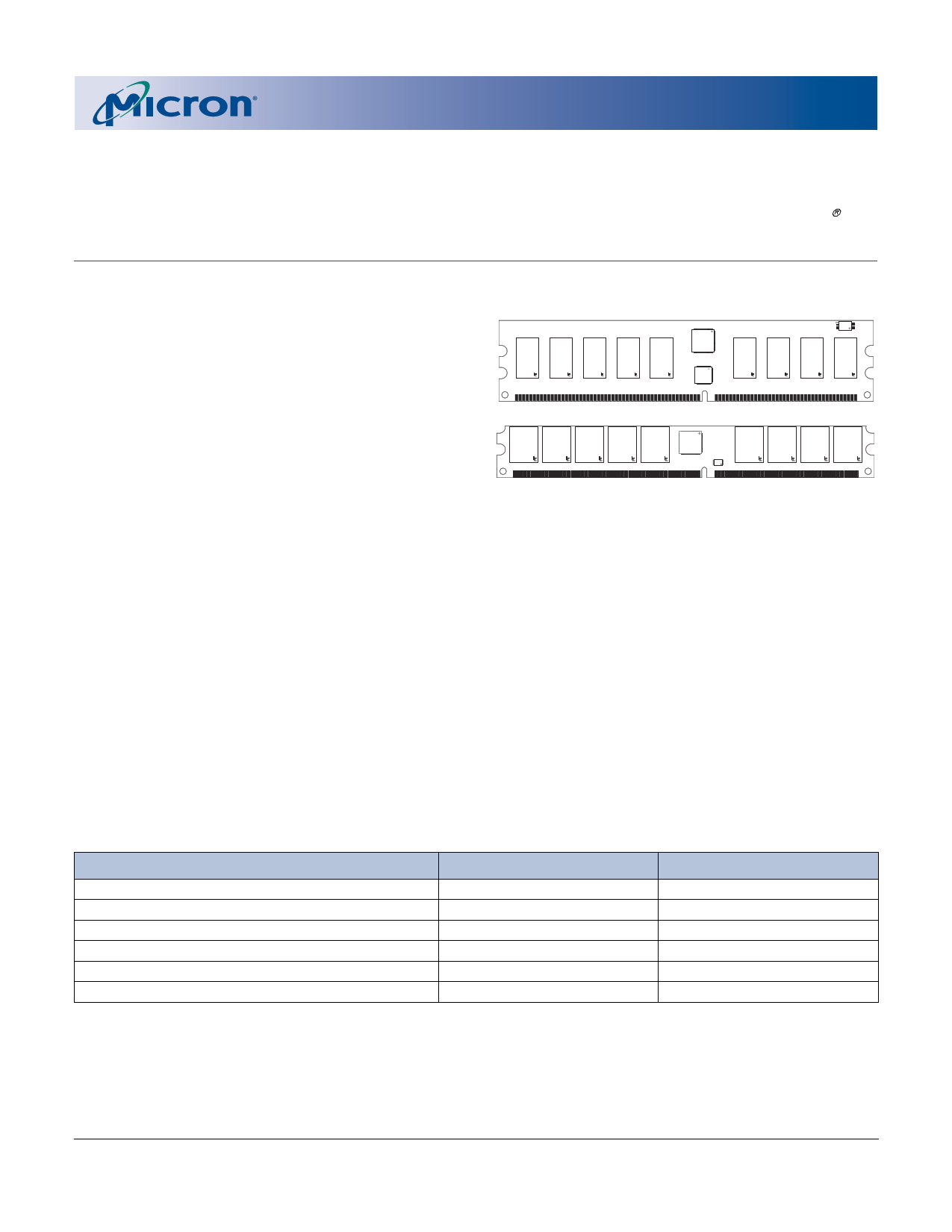
Figure 1: 184-Pin DIMM (MO-206)
Low-Profile 1.125in. (28.58mm)
Very Low Profile 0.72in. (18.29mm)
OPTIONS
• Operating Temperature Range
Commercial (0°C ≤ TA ≤ +70°C)
• Package
184-pin DIMM (standard)
184-pin DIMM (lead-free)1
• Memory Clock, Speed, CAS Latency2
5ns (200 MHz), 400 MT/s, CL = 3
• PCB
1.125in (28.58mm)
MARKING
none
G
Y
-40B
NOTE: 1. Contact Micron for availability of products.
2. CL = CAS latency; registered Mode adds one
clock cycle to CL.
Table 1: Address Table
Refresh Count
Row Addressing
Device Bank Addressing
Device Configuration
Column Addressing
Module Rank Addressing
512MB
8K
8K (A0–A12)
4 (BA0, BA1)
256Mb (64 Meg x 4)
2K (A0–A9, A11)
1 (S0#)
1GB
8K
8K (A0–A12)
4 (BA0, BA1)
512Mb (128 Meg x 4)
4K (A0–A9, A11, A12)
1 (S0#)
1pdf: 09005aef80f6b913, source: 09005aef80f6b41c
DDAF18C64_128x72G.fm - Rev. C 9/04 EN
©2004 Micron Technology, Inc. All rights reserved.
PRODUCTS AND SPECIFICATIONS DISCUSSED HEREIN ARE SUBJECT TO CHANGE BY MICRON WITHOUT NOTICE.
1 page 
512MB, 1GB (x72, ECC, SR) PC3200
184-PIN DDR SDRAM RDIMM
Table 5: Pin Descriptions
Pin numbers may not correlate with symbol; refer to Pin Assignment Tables for pin number and symbol information.
PIN NUMBERS
2, 4, 6, 8, 12,13, 19, 20,
23, 24, 28, 31, 33, 35, 39,
40, 53, 55, 57, 60, 61, 64,
68, 69, 72, 73, 79, 80, 83,
84, 87, 88, 94, 95, 98, 99,
105, 106, 109, 110, 114,
117, 121, 123, 126, 127,
131, 133, 146, 147, 150,
151, 153, 155, 161, 162,
165, 166, 170, 171, 174,
175, 178, 179
92
181, 182, 183
91
1
15, 22, 30, 54, 62, 77, 96,
104, 112, 128, 136, 143,
156, 164, 172, 180
7, 38, 46, 70, 85, 108,
120, 148, 168
3, 11, 18, 26, 34, 42, 50,
58, 66, 74, 81, 89, 93, 100,
116, 124, 132, 139, 145,
152, 160, 176
184
9, 16, 17, 71, 75, 76, 82,
90, 101, 102, 103, 111,
113,158, 163, 167, 173
SYMBOL
DQ0–DQ63
SCL
SA0–SA2
SDA
VREF
VDDQ
VDD
VSS
VDDSPD
NC
TYPE
Input/ Data I/Os: Data bus.
Output
DESCRIPTION
Input Serial Clock for Presence-Detect: SCL is used to synchronize the
presence-detect data transfer to and from the module.
Input Presence-Detect Address Inputs: These pins are used to
configure the presence-detect device.
Input/ Serial Presence-Detect Data: SDA is a bidirectional pin used to
Output transfer addresses and data into and out of the presence-detect
portion of the module.
Supply SSTL_2 reference voltage.
Supply DQ Power Supply: +2.6V ±0.1V.
Supply Power Supply: +2.6V ±0.1V.
Supply Ground.
Supply Serial EEPROM positive power supply: +2.3V to +3.6V.
— No Connect: These pins should be left unconnected.
pdf: 09005aef80f6b913, source: 09005aef80f6b41c
DDAF18C64_128x72G.fm - Rev. C 9/04 EN
5 Micron Technology, Inc., reserves the right to change products or specifications without notice.
©2004 Micron Technology, Inc. All rights reserved.
5 Page 
512MB, 1GB (x72, ECC, SR) PC3200
184-PIN DDR SDRAM RDIMM
to zero, bit A8 set to one, and bits A0–A6 set to the
desired values. Although not required by the Micron
device, JEDEC specifications recommend when a
LOAD MODE REGISTER command is issued to reset
the DLL, it should always be followed by a LOAD
MODE REGISTER command to select normal operat-
ing mode.
All other combinations of values for A7–A12 are
reserved for future use and/or test modes. Test modes
and reserved states should not be used because
unknown operation or incompatibility with future ver-
sions may result.
Extended Mode Register
The extended mode register controls functions
beyond those controlled by the mode register; these
additional functions are DLL enable/disable and out-
put drive strength. These functions are controlled via
the bits shown in the Extended Mode Register Defini-
tion Diagram. The extended mode register is pro-
grammed via the LOAD MODE REGISTER command
to the mode register (with BA0 = 1 and BA1 = 0) and
will retain the stored information until it is pro-
grammed again or the device loses power. The
enabling of the DLL should always be followed by a
LOAD MODE REGISTER command to the mode regis-
ter (BA0/BA1 both LOW) to reset the DLL.
The extended mode register must be loaded when
all device banks are idle and no bursts are in progress,
and the controller must wait the specified time before
initiating any subsequent operation. Violating either
of these requirements could result in unspecified oper-
ation.
DLL Enable/Disable
The DLL must be enabled for normal operation.
DLL enable is required during power-up initialization
and upon returning to normal operation after having
disabled the DLL for the purpose of debug or evalua-
tion. (When the device exits self refresh mode, the DLL
is enabled automatically.) Any time the DLL is enabled,
a DLL Reset and 200 clock cycles with CKE HIGH must
occur before a READ command can be issued.
Figure 7: Extended Mode Register
Definition Diagram
BA1 BA0 A12 A11 A10 A9 A8 A7 A6 A5 A4 A3 A2 A1 A0 Address Bus
14 13 12 11 10 9 8 7 6 5 4 3 2 1 0 Extended Mode
01 11
Operating Mode
DS DLL Register (Ex)
E0 DLL
0 Enable
1 Disable
E1 Drive Strength
0 Normal
E12 E11 E10 E9 E8 E7 E6 E5 E4 E3 E22
0 0 0 0 0 0 00 0 0 0
– – – – – – –– – – –
E1, E0
Valid
–
Operating Mode
Reserved
Reserved
NOTE:
1. BA1 and BA0 (E14 and E13) must be “0, 1” to select the
Extended Mode Register (vs. the base Mode Register).
2. QFC# is not supported.
pdf: 09005aef80f6b913, source: 09005aef80f6b41c
DDAF18C64_128x72G.fm - Rev. C 9/04 EN
11
Micron Technology, Inc., reserves the right to change products or specifications without notice.
©2004 Micron Technology, Inc. All rights reserved.
11 Page | ||
| Páginas | Total 30 Páginas | |
| PDF Descargar | [ Datasheet MT18VDDF12872.PDF ] | |
Hoja de datos destacado
| Número de pieza | Descripción | Fabricantes |
| MT18VDDF12872 | 1GB DDR SDRAM REGISTERED DIMM | Micron |
| MT18VDDF12872H | 1GB DDR SDRAM SODIMM | Micron |
| Número de pieza | Descripción | Fabricantes |
| SLA6805M | High Voltage 3 phase Motor Driver IC. |
Sanken |
| SDC1742 | 12- and 14-Bit Hybrid Synchro / Resolver-to-Digital Converters. |
Analog Devices |
|
DataSheet.es es una pagina web que funciona como un repositorio de manuales o hoja de datos de muchos de los productos más populares, |
| DataSheet.es | 2020 | Privacy Policy | Contacto | Buscar |