|
|
|
PDF MT9VDDF3272 Data sheet ( Hoja de datos )
| Número de pieza | MT9VDDF3272 | |
| Descripción | 256MB DDR SDRAM REGISTERED DIMM | |
| Fabricantes | Micron | |
| Logotipo | ||
Hay una vista previa y un enlace de descarga de MT9VDDF3272 (archivo pdf) en la parte inferior de esta página. Total 30 Páginas | ||
|
No Preview Available !
DDR SDRAM
REGISTERED DIMM
256MB, 512MB (x72, ECC, SR)
184-PIN DDR SDRAM RDIMM
MT9VDDF3272 – 256MB
MT9VDDF6472 – 512MB
For the latest data sheet, please refer to the Micron Web
site: www.micron.com/products/modules
Features
• 184-pin, dual, in-line memory module (DIMM)
• Fast data transfer rates: PC1600, PC2100, or PC2700
• Utilizes 200 MT/s, 266 MT/s, and 333 MT/s DDR
SDRAM components
• Registered Inputs with one-clock delay
• Phase-lock loop (PLL) clock driver to reduce loading
• Supports ECC error detection and correction
• 256MB (32 Meg x 72); and 512MB (64 Meg x 72)
• VDD = VDDQ = +2.5V
• VDDSPD = +2.3V to +3.6V
• 2.5V I/O (SSTL_2 compatible)
• Commands entered on each positive CK edge
• DQS edge-aligned with data for READs; center-
aligned with data for WRITEs
• Internal, pipelined double data rate (DDR)
architecture; two data accesses per clock cycle
• Bidirectional data strobe (DQS) transmitted/received
with data—i.e., source-synchronous data capture
• Differential clock inputs CK and CK#
• Four internal device banks for concurrent operation
• Programmable burst lengths: 2, 4, or 8
• Auto precharge option
• Auto Refresh and Self Refresh Modes
• 7.8125µs maximum average periodic refresh
interval
• Serial Presence-Detect (SPD) with EEPROM
• Programmable READ CAS latency
• Gold edge contacts
OPTIONS
• Operating Temperature Range
Commercial (0°C ≤ TA ≤ +70°C)
Industrial (-40°C ≤ TA ≤ +85°C)
MARKING
none
I1
Table 1: Address Table
Refresh Count
Row Addressing
Device Bank Addressing
Device Configuration
Column Addressing
Module Rank Addressing
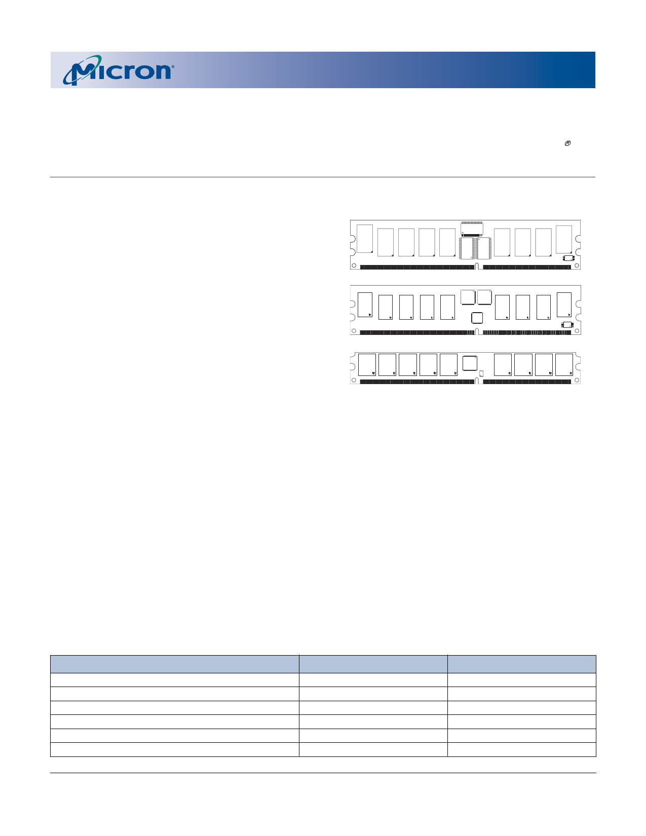
Figure 1: 184-Pin DIMM (MO-206)
Low-Profile 1.125in. (28.58mm) 256MB
Low-Profile 1.125in. (28.58mm) 512MB
Very Low-Profile 0.72in. (18.29mm)
OPTIONS
• Package
184-pin DIMM (standard)
184-pin DIMM (lead-free)1
• Memory Clock, Speed, CAS Latency2
6ns (167 MHz), 333 MT/s, CL = 2.5
7.5ns (133 MHz), 266 MT/s, CL = 2
7.5ns (133 MHz), 266 MT/s, CL = 2
7.5ns (133 MHz), 266 MT/s, CL = 2.5
10ns (100 MHz), 200 MT/s, CL = 2
• PCB
Low-Profile 1.125in. (28.58mm)
Very Low-Profile 0.72in. (18.29mm)
MARKING
G
Y
-335
-2621
-26A1
-265
-202
NOTE: 1. Contact Micron for product availability.
2. CL = CAS (READ) Latency; Registered mode will
add one clock cycle to CL.
256MB
8K
8K (A0–A12)
4 (BA0, BA1)
256Mb (32 Meg x 8)
1K (A0–A9)
1 (S0#)
512MB
8K
8K (A0–A12)
4 (BA0, BA1)
512Mb (64 Meg x 8)
2K (A0–A9, A11)
1 (S0#)
pdf: 09005aef80e119b2, source: 09005aef807d56a1
DDF9C32_64x72G.fm - Rev. B 9/04 EN
1
©2004 Micron Technology, Inc. All rights reserved.
PRODUCTS AND SPECIFICATIONS DISCUSSED HEREIN ARE SUBJECT TO CHANGE BY MICRON WITHOUT NOTICE.
1 page 
256MB, 512MB (x72, ECC, SR)
184-PIN DDR SDRAM RDIMM
Table 5: Pin Descriptions
Pin numbers may not correlate with symbols. Refer to Pin Assignment tables on page 3 for more information
PIN NUMBERS
2, 4, 6, 8, 12,13, 19, 20,
23, 24, 28, 31, 33, 35, 39,
40, 53, 55, 57, 60, 61, 64,
68, 69, 72, 73, 79, 80, 83,
84, 87, 88, 94, 95, 98, 99,
105, 106, 109, 110, 114,
117, 121, 123, 126, 127,
131, 133, 146, 147, 150,
151, 153, 155, 161, 162,
165, 166, 170, 171, 174,
175, 178, 179
92
181, 182, 183
91
1
15, 22, 30, 54, 62, 77, 96,
104, 112, 128, 136, 143,
156, 164, 172, 180
7, 38, 46, 70, 85, 108, 120,
148, 168
3, 11, 18, 26, 34, 42, 50,
58, 66, 74, 81, 89, 93, 100,
116, 124, 132, 139, 145,
152, 160, 176
184
16, 17, 75, 76, 90, 111,
158
9, 71, 82, 101, 102, 103,
113, 163, 167, 173
SYMBOL
DQ0–DQ63
SCL
SA0–SA2
SDA
VREF
VDDQ
VDD
VSS
VDDSPD
DNU
NC
TYPE
Input/ Data I/Os: Data bus.
Output
DESCRIPTION
Input Serial Clock for Presence-Detect: SCL is used to synchronize the
presence-detect data transfer to and from the module.
Input Presence-Detect Address Inputs: These pins are used to
configure the presence-detect device.
Input/ Serial Presence-Detect Data: SDA is a bidirectional pin used to
Output transfer addresses and data into and out of the presence-detect
portion of the module.
Supply SSTL_2 reference voltage.
Supply DQ Power Supply: +2.5V ±0.2V.
Supply Power Supply: +2.5V ±0.2V.
Supply Ground.
Supply
—
—
Serial EEPROM positive power supply: .
Do Not Use: Thes pins are not connected on these modules, but
are assigned pins on other modules in this product family
No Connect: These pins should be left unconnected.
pdf: 09005aef80e119b2, source: 09005aef807d56a1
DDF9C32_64x72G.fm - Rev. B 9/04 EN
5 Micron Technology, Inc., reserves the right to change products or specifications without notice.
©2004 Micron Technology, Inc. All rights reserved.
5 Page 
Table 6: Burst Definition Table
BURST
LENGTH
STARTING
COLUMN
ADDRESS
ORDER OF ACCESSES WITHIN
A BURST
TYPE =
TYPE =
SEQUENTIAL INTERLEAVED
A0
2
0 0-1
0-1
1 1-0
1-0
A1 A0
00
0-1-2-3
0-1-2-3
4
01
1-2-3-0
1-0-3-2
10
2-3-0-1
2-3-0-1
11
A2 A1 A0
3-0-1-2
3-2-1-0
0 0 0 0-1-2-3-4-5-6-7 0-1-2-3-4-5-6-7
0 0 1 1-2-3-4-5-6-7-0 1-0-3-2-5-4-7-6
8 0 1 0 2-3-4-5-6-7-0-1 2-3-0-1-6-7-4-5
0 1 1 3-4-5-6-7-0-1-2 3-2-1-0-7-6-5-4
1 0 0 4-5-6-7-0-1-2-3 4-5-6-7-0-1-2-3
1 0 1 5-6-7-0-1-2-3-4 5-4-7-6-1-0-3-2
1 1 0 6-7-0-1-2-3-4-5 6-7-4-5-2-3-0-1
1 1 1 7-0-1-2-3-4-5-6 7-6-5-4-3-2-1-0
NOTE:
1. For a burst length of two, A1–Ai select the two-data-
element block; A0 selects the first access within the
block.
2. For a burst length of four, A2–Ai select the four-data-
element block; A0–A1 select the first access within the
block.
3. For a burst length of eight, A3–Ai select the eight-data-
element block; A0–A2 select the first access within the
block.
4. Whenever a boundary of the block is reached within a
given sequence above, the following access wraps
within the block.
5. i = 9 for 256MB,
i = 9, 11 for 512MB
Table 7: CAS Latency Table
SPEED
-335
-262
-26A
-265
-202
ALLOWABLE OPERATING
CLOCK FREQUENCY (MHZ)
CL = 2
75 ≤ f ≤ 133
75 ≤ f ≤ 133
75 ≤ f ≤ 133
75 ≤ f ≤ 100
75 ≤ f ≤ 100
CL = 2.5
75 ≤ f ≤ 167
75 ≤ f ≤ 133
75 ≤ f ≤ 133
75 ≤ f ≤ 133
75 ≤ f ≤ 125
256MB, 512MB (x72, ECC, SR)
184-PIN DDR SDRAM RDIMM
Figure 7: CAS Latency Diagram
CK#
CK
COMMAND
T0
READ
DQS
DQ
T1
NOP
CL = 2
T2 T2n
T3 T3n
NOP NOP
CK#
CK
COMMAND
T0
READ
DQS
DQ
T1 T2 T2n T3 T3n
NOP
CL = 2.5
NOP
NOP
Burst Length = 4 in the cases shown
Shown with nominal tAC, tDQSCK, and tDQSQ
TRANSITIONING DATA
DON’T CARE
Operating Mode
The normal operating mode is selected by issuing a
MODE REGISTER SET command with bits A7–A12
each set to zero, and bits A0–A6 set to the desired val-
ues. A DLL reset is initiated by issuing a MODE REGIS-
TER SET command with bits A7 and A9–A12 each set
to zero, bit A8 set to one, and bits A0–A6 set to the
desired values. Although not required by the Micron
device, JEDEC specifications recommend when a
LOAD MODE REGISTER command is issued to reset
the DLL, it should always be followed by a LOAD
MODE REGISTER command to select normal operat-
ing mode.
All other combinations of values for A7–A12 are
reserved for future use and/or test modes. Test modes
and reserved states should not be used because
unknown operation or incompatibility with future ver-
sions may result.
Extended Mode Register
The extended mode register controls functions
beyond those controlled by the mode register; these
additional functions are DLL enable/disable and out-
put drive strength. These functions are controlled via
the bits shown in Figure 8, Extended Mode Register
Definition Diagram. The extended mode register is
programmed via the LOAD MODE REGISTER com-
mand to the mode register (with BA0 = 1 and BA1 = 0)
pdf: 09005aef80e119b2, source: 09005aef807d56a1
DDF9C32_64x72G.fm - Rev. B 9/04 EN
11
Micron Technology, Inc., reserves the right to change products or specifications without notice.
©2004 Micron Technology, Inc. All rights reserved.
11 Page | ||
| Páginas | Total 30 Páginas | |
| PDF Descargar | [ Datasheet MT9VDDF3272.PDF ] | |
Hoja de datos destacado
| Número de pieza | Descripción | Fabricantes |
| MT9VDDF3272 | 256MB DDR SDRAM REGISTERED DIMM | Micron |
| Número de pieza | Descripción | Fabricantes |
| SLA6805M | High Voltage 3 phase Motor Driver IC. |
Sanken |
| SDC1742 | 12- and 14-Bit Hybrid Synchro / Resolver-to-Digital Converters. |
Analog Devices |
|
DataSheet.es es una pagina web que funciona como un repositorio de manuales o hoja de datos de muchos de los productos más populares, |
| DataSheet.es | 2020 | Privacy Policy | Contacto | Buscar |