|
|
|
PDF AT49LW080-33JC Data sheet ( Hoja de datos )
| Número de pieza | AT49LW080-33JC | |
| Descripción | 8-megabit and 4-megabit Firmware Hub Flash Memory | |
| Fabricantes | ATMEL Corporation | |
| Logotipo | ||
Hay una vista previa y un enlace de descarga de AT49LW080-33JC (archivo pdf) en la parte inferior de esta página. Total 30 Páginas | ||
|
No Preview Available !
Features
• Low Pin Count (LPC) BIOS Device
• Functions as Firmware Hub for Intel 810, 810E, 820, 840 Chipsets
• 8M or 4M Bits of Flash Memory for Platform Code/Data Storage
– Uniform, 64-Kbyte Memory Sectors
– Available in 8M Bits (AT49LW080) and 4M Bits (AT49LW040)
– Automated Byte-program and Sector-erase Operations
• Two Configurable Interfaces
– Firmware Hub (FWH) Interface for In-System Operation
– Address/Address Multiplexed (A/A Mux) Interface for Programming during
Manufacturing
• Firmware Hub Hardware Interface Mode
– 5-signal Communication Interface Supporting x8 Reads and Writes
– Read and Write Protection for Each Sector Using Software-controlled Registers
– Two Hardware Write-protect Pins: One for the Top Boot Sector, One for All Other
Sectors
– Five General-purpose Inputs, GPIs, for Platform Design Flexibility
– Operates with 33 MHz PCI Clock and 3.3V I/O
• Address/Address Multiplexed (A/A Mux) Interface
– 11-pin Multiplexed Address and 8-pin Data Interface
– Supports Fast On-board or Out-of-system Programming
• Power Supply Specifications
– VCC: 3.3V ± 0.3V
– VPP: 3.3V and 12V for Fast Programming
• Industry-standard Packages
– (40-lead TSOP or 32-lead PLCC)
Description
The AT49LW080 and the AT49LW040 are Flash memory devices designed to be com-
patible with the Intel 82802AC and the Intel 82802AB Firmware Hub (FWH) devices
for PC-Bios Application. A feature of the AT49LW080/040 is the nonvolatile memory
core. The high-performance memory is arranged in eight (AT49LW040) or sixteen
(AT49LW080) 64-Kbyte sectors (see page 13).
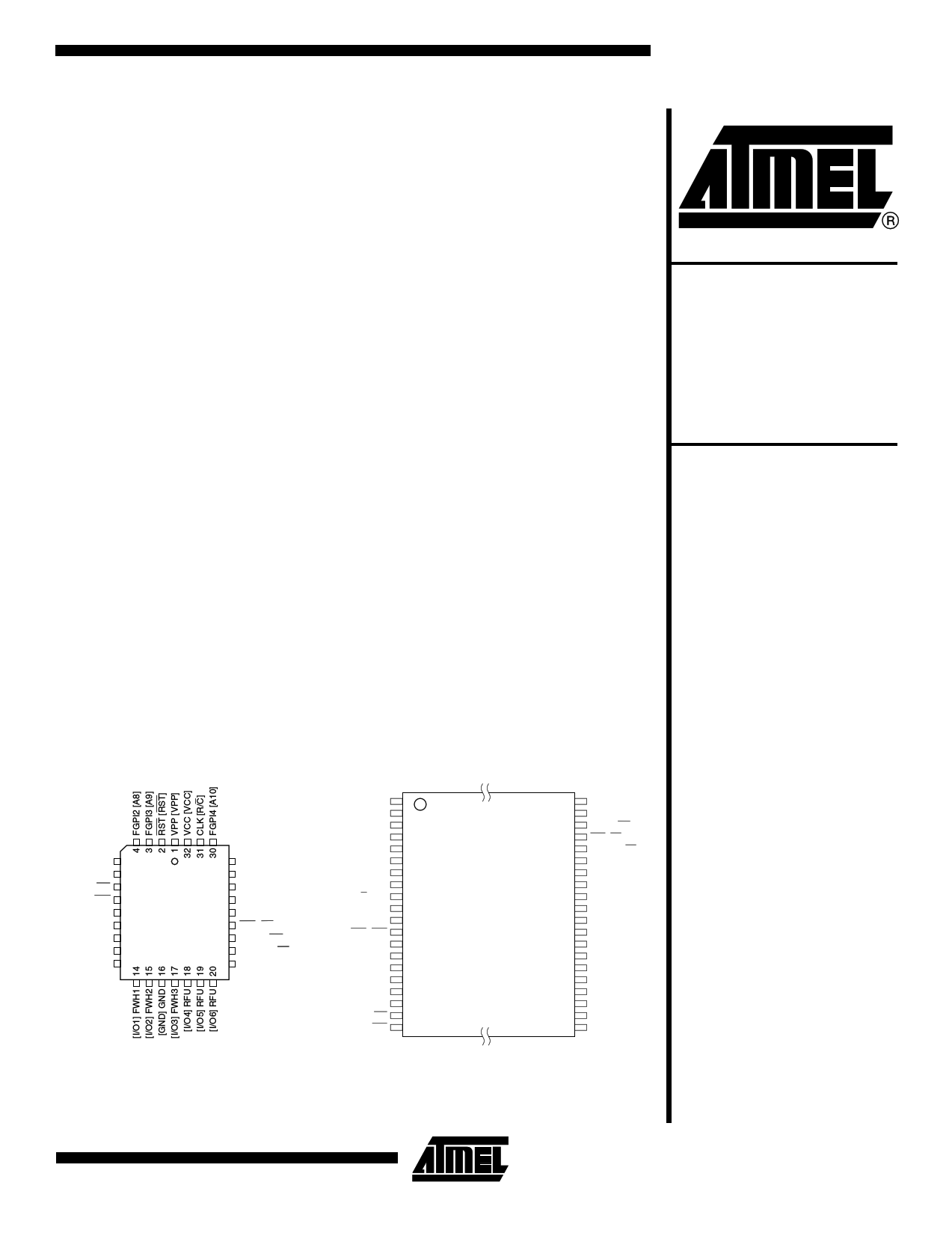
Pin Configurations
PLCC
TSOP
[A7] FGPI1
[A6] FGPI0
[A5] WP
[A4] TBL
[A3] ID3
[A2] ID2
[A1] ID1
[A0] ID0
[I/O0] FWH0
5
6
7
8
9
10
11
12
13
29 IC (VIL) [IC(VIH)]
28 GNDa [GNDa]
27 VCCa [VCCa]
26 GND [GND]
25 VCC [VCC]
24 INIT [OE]
23 FWH4 [WE]
22 RFU [RY/BY]
21 RFU [I/O7]
(NC) NC
[IC (VIH)] IC (VIL)
[NC] NC
[NC] NC
[NC] NC
[NC] NC
[A10] FGPI4
[NC] NC
[R/C] CLK
[VCC] VCC
[VPP] VPP
[RST] RST
[NC] NC
[NC] NC
[A9] FGPI3
[A8] FGPI2
[A7] FGPI1
[A6] FGPI0
[A5] WP
[A4] TBL
1
2
3
4
5
6
7
8
9
10
11
12
13
14
15
16
17
18
19
20
40 GNDa [GNDa]
39 VCCa [VCCa]
38 FWH4 [WE]
37 INIT [OE]
36 RFU [RY/BY]
35 RFU [I/O7]
34 RFU [I/O6]
33 RFU [I/O5]
32 RFU [I/O4]
31 VCC [VCC]
30 GND [GND]
29 GND [GND]
28 FWH3 [I/O3]
27 FWH2 [I/O2]
26 FWH1 [I/O1]
25 FWH0 [I/O0]
24 ID0 [A0]
23 ID1 [A1]
22 ID2 [A2]
21 ID3 [A3]
[ ] Designates A/A Mux Mode
[ ] Designates A/A Mux Mode
8-megabit and
4-megabit
Firmware Hub
Flash Memory
AT49LW080
AT49LW040
Rev. 1966C–FLASH–03/02
1
1 page 
AT49LW080/040
Table 1. Pin Description (Continued)
Interface
Symbol
Type
FWH A/A Mux
I/O0 - I/O7
I/O
X
OE INPUT
R/C INPUT
X
X
WE INPUT
X
VPP
SUPPLY
X
X
VCC
GND
VCCa
GNDa
RFU
NC
RY/BY
SUPPLY
X
X
SUPPLY
SUPPLY
SUPPLY
X
X
X
X
X
X
X
X
OUTPUT
X
X
Name and Function
DATA INPUT/OUTPUTS: These pins receive data and commands during
write cycles and transmit data during memory array and identifier code
read cycles. Data pins float to high-impedance when the chip is
deselected or outputs are disabled. Data is internally latched during a
write cycle.
OUTPUT ENABLE: Gates the device’s outputs during a read cycle.
ROW-COLUMN ADDRESS SELECT: For the A/A Mux interface, this pin
determines whether the address pins are pointing to the row addresses,
A0 - A10, or to the column addresses, A11 - A18 (AT49LW040) or
A11 - A19 (AT49LW080).
WRITE ENABLE: Controls writes to the array sectors. Addresses and
data are latched on the rising edge of the WE pulse.
SECTOR ERASE/PROGRAM POWER SUPPLY: For erasing array
sectors or programming data. VPP = 3.3V or 12V. With VPP ≤ VPPLK,
memory contents cannot be altered. Sector erase or program with an
invalid VPP (see DC Characteristics) produces spurious results and
should not be attempted. VPP may only be held at 12V for 80 hours over
the lifetime of the device.
DEVICE POWER SUPPLY: Internal detection automatically configures
the device for optimized read performance. Do no float any power pins.
With VCC ≤ VLKO, all write attempts to the flash memory are inhibited.
Device operations at invalid VCC voltages (see DC Characteristics)
produce spurious results and should not be attempted.
GROUND: Do not float any ground pins.
ANALOG POWER SUPPLY: This supply should share the same system
supply as VCC.
ANALOG GROUND: Should be tied to same plane as GND.
RESERVED FOR FUTURE USE: These pins are reserved for future
generations of this product and should be connected accordingly. These
pins may be left disconnected or driven. If they are driven, the voltage
levels should meet VIH and VIL requirements.
A/A Mux = I/O[7:4]
NO CONNECT: Pin may be driven or floated. If it is driven, the voltage
levels should meet VIH and VIL. No connects appear only on the 40-lead
TSOP package.
READY/BUSY: Valid only in A/A Mux Mode. This output pin is a reflection
of bit 7 in the status register. This pin is used to determine sector erase or
program completion.
1966C–FLASH–03/02
5
5 Page 
Response to Invalid
Fields
Bus Abort
AT49LW080/040
OUTPUT DISABLE: When the FWH is not selected through a FWH read or write cycle,
the FWH interface outputs (FWH[3:0]) are disabled and will be placed in a high-imped-
ance state.
During FWH operations, the FWH will not explicitly indicate that it has received invalid
field sequences. The response to specific invalid fields or sequences is as follows:
• Address out of range: The FWH address sequences is seven fields long (28 bits),
but only the last five address fields (20 bits) will be decoded by an 8-Mbit FWH. (For
a 4-Mbit density, the most significant bit (FWH3) in the third address field also will be
ignored.) The FWH will respond to these lower addresses, regardless of the value of
the more-significant address bits. Address A22 has the special function of directing
reads and writes to the Flash core (A22 = 1) or to the register space (A22 = 0).
• Invalid MSIZE field: If the FWH receives an invalid size field during a read or write
operation, the internal state machine will reset and no operation will be attempted.
The FWH will generate no response of any kind in this situation. Invalid-size fields
for a read cycle are anything but 0000. Invalid-size fields for a write cycle are
anything but 0000. When accessing register space, invalid field sizes are anything
but 0000.
Once valid START, IDSEL, and MSIZE fields are received, the FWH always will
respond to subsequent inputs as if they were valid. As long as the states of FWH
[3:0] and FWH4 are known, the response of the FWH to signals received during the
FWH cycle should be predictable. The FWH will make no attempt to check the valid-
ity of incoming Flash operation commands.
The Bus Abort operation can be used to immediately abort the current bus operation. A
Bus Abort occurs when FWH4 is driven Low, VIL, during the bus operation; the memory
will tri-state the Input/Output Communication pins, FWH3 - FWH0 and the FWH state
machine will reset. During a write cycle, there is the possibility that an internal Flash
write or erase operation is in progress (or has just been initiated). If the FWH4 is
asserted during this time frame, the internal operation will not abort. The software must
send an explicit Flash command to terminate or suspend the operation. The internal
FWH state machine will not initiate a Flash write or erase operation until it has received
the last nibble from the chipset. This means that FWH4 can be asserted as late as cycle
12 (Table 6) and no internal Flash operation will be attempted.
HARDWARE WRITE-PROTECT PINS TBL AND WP: Two pins are available with the
FWH to provide hardware write-protect capabilities.
The Top Sector Lock (TBL) pin is a signal, when held low (active), prevents program or
sector erase operations in the top sector of the device (sector 7 – AT49LW040 and sec-
tor 15 – AT49LW080) where critical code can be stored. When TBL is high, hardware
write protection of the top sector is disabled. The write-protect (WP) pin serves the same
function for all the remaining sectors except the top sector. WP operates independently
from TBL and does not affect the lock status of the top sector.
The TBL and WP pins must be set to the desired protection state prior to starting a pro-
gram or erase operation since they are sampled at the beginning of the operation.
Changing the state of TBL or WP during a program or erase operation may cause
unpredictable results.
1966C–FLASH–03/02
11
11 Page | ||
| Páginas | Total 30 Páginas | |
| PDF Descargar | [ Datasheet AT49LW080-33JC.PDF ] | |
Hoja de datos destacado
| Número de pieza | Descripción | Fabricantes |
| AT49LW080-33JC | 8-megabit and 4-megabit Firmware Hub Flash Memory | ATMEL Corporation |
| Número de pieza | Descripción | Fabricantes |
| SLA6805M | High Voltage 3 phase Motor Driver IC. |
Sanken |
| SDC1742 | 12- and 14-Bit Hybrid Synchro / Resolver-to-Digital Converters. |
Analog Devices |
|
DataSheet.es es una pagina web que funciona como un repositorio de manuales o hoja de datos de muchos de los productos más populares, |
| DataSheet.es | 2020 | Privacy Policy | Contacto | Buscar |