|
|
|
PDF AT89C1051 Data sheet ( Hoja de datos )
| Número de pieza | AT89C1051 | |
| Descripción | 8-Bit Microcontroller with 1K Byte Flash | |
| Fabricantes | ATMEL Corporation | |
| Logotipo | ||
Hay una vista previa y un enlace de descarga de AT89C1051 (archivo pdf) en la parte inferior de esta página. Total 12 Páginas | ||
|
No Preview Available !
Features
• Compatible with MCS-51™ Products
• 1K Byte of Reprogrammable Flash Memory
– Endurance: 1,000 Write/Erase Cycles
• 2.7V to 6V Operating Range
• Fully Static Operation: 0 Hz to 24 MHz
• Two-Level Program Memory Lock
• 64 bytes SRAM
• 15 Programmable I/O Lines
• One 16-Bit Timer/Counter
• Three Interrupt Sources
• Direct LED Drive Outputs
• On-Chip Analog Comparator
• Low Power Idle and Power Down Modes
Description
The AT89C1051 is a low-voltage, high-performance CMOS 8-bit microcomputer with
1K byte of Flash programmable and erasable read only memory (PEROM). The
device is manufactured using Atmel’s high density nonvolatile memory technology
and is compatible with the industry standard MCS-51™ instruction set. By combining
a versatile 8-bit CPU with Flash on a monolithic chip, the Atmel AT89C1051 is a pow-
erful microcomputer which provides a highly flexible and cost effective solution to
many embedded control applications.
The AT89C1051 provides the following standard features: 1K Byte of Flash, 64 bytes
of RAM, 15 I/O lines, one 16-bit timer/counter, a three vector two-level interrupt archi-
tecture, a precision analog comparator, on-chip oscillator and clock circuitry. In addi-
tion, the AT89C1051 is designed with static logic for operation down to zero frequency
and supports two software selectable power saving modes. The Idle Mode stops the
CPU while allowing the RAM, timer/counters, serial port and interrupt system to con-
tinue functioning. The Power Down Mode saves the RAM contents but freezes the
oscillator disabling all other chip functions until the next hardware reset.
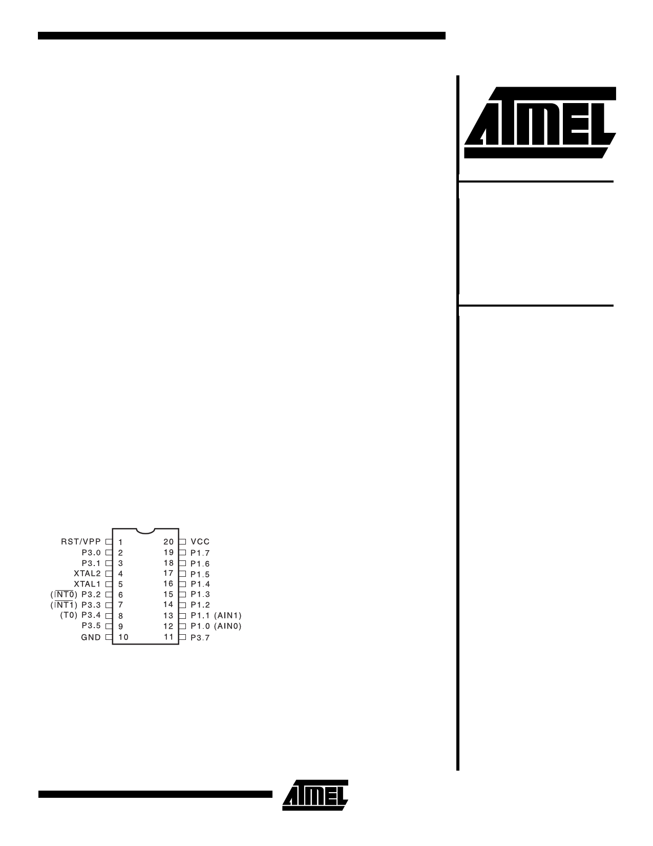
Pin Configuration
PDIP/SOIC
8-Bit
Microcontroller
with 1K Byte
Flash
AT89C1051
0366D-A–12/97
4-3
1 page 
AT89C1051
1. Branching instructions:
LCALL, LJMP, ACALL, AJMP, SJMP, JMP @A+DPTR
These unconditional branching instructions will execute
correctly as long as the programmer keeps in mind that the
destination branching address must fall within the physical
boundaries of the program memory size (locations 00H to
3FFH for the 89C1051). Violating the physical space limits
may cause unknown program behavior.
CJNE [...], DJNZ [...], JB, JNB, JC, JNC, JBC, JZ, JNZ With
these conditional branching instructions the same rule
above applies. Again, violating the memory boundaries
may cause erratic execution.
For applications involving interrupts the normal interrupt
service routine address locations of the 80C51 family archi-
tecture have been preserved.
2. MOVX-related instructions, Data Memory:
The AT89C1051 contains 64 bytes of internal data mem-
ory. Thus, in the AT89C1051 the stack depth is limited to
64 bytes, the amount of available RAM. External DATA
memory access is not supported in this device, nor is exter-
nal PROGRAM memory execution. Therefore, no MOVX
[...] instructions should be included in the program.
A typical 80C51 assembler will still assemble instructions,
even if they are written in violation of the restrictions men-
tioned above. It is the responsibility of the controller user to
know the physical features and limitations of the device
being used and adjust the instructions used correspond-
ingly.
Program Memory Lock Bits
On the chip are two lock bits which can be left unpro-
grammed (U) or can be programmed (P) to obtain the addi-
tional features listed in the table below:
Lock Bit Protection Modes(1)
Program Lock Bits
LB1 LB2 Protection Type
1 U U No program lock features.
2 P U Further programming of the Flash
is disabled.
3
Note:
P P Same as mode 2, also verify is
disabled.
1. The Lock Bits can only be erased with the Chip Erase
operation.
Idle Mode
In idle mode, the CPU puts itself to sleep while all the on-
chip peripherals remain active. The mode is invoked by
software. The content of the on-chip RAM and all the spe-
cial functions registers remain unchanged during this
mode. The idle mode can be terminated by any enabled
interrupt or by a hardware reset.
P1.0 and P1.1 should be set to ‘0’ if no external pullups are
used, or set to ‘1’ if external pullups are used.
It should be noted that when idle is terminated by a hard-
ware reset, the device normally resumes program execu-
tion, from where it left off, up to two machine cycles before
the internal reset algorithm takes control. On-chip hardware
inhibits access to internal RAM in this event, but access to
the port pins is not inhibited. To eliminate the possibility of
an unexpected write to a port pin when Idle is terminated by
reset, the instruction following the one that invokes Idle
should not be one that writes to a port pin or to external
memory.
Power Down Mode
In the power down mode the oscillator is stopped, and the
instruction that invokes power down is the last instruction
executed. The on-chip RAM and Special Function Regis-
ters retain their values until the power down mode is termi-
nated. The only exit from power down is a hardware reset.
Reset redefines the SFRs but does not change the on-chip
RAM. The reset should not be activated before VCC is
restored to its normal operating level and must be held
active long enough to allow the oscillator to restart and sta-
bilize.
P1.0 and P1.1 should be set to ’0’ if no external pullups are
used, or set to ’1’ if external pullups are used.
Programming The Flash
The AT89C1051 is shipped with the 1K byte of on-chip
PEROM code memory array in the erased state (i.e., con-
tents = FFH) and ready to be programmed. The code mem-
ory array is programmed one byte at a time. Once the array
is programmed, to re-program any non-blank byte, the
entire memory array needs to be erased electrically.
Internal Address Counter: The AT89C1051 contains an
internal PEROM address counter which is always reset to
000H on the rising edge of RST and is advanced by apply-
ing a positive going pulse to pin XTAL1.
4-7
5 Page 
AT89C1051
20
I 15
C
C 10
m
A5
0
0
AT89C1051
TYPICAL ICC - ACTIVE (85°C)
Vc c= 6.0V
Vc c= 5.0V
Vc c= 3.0V
6 12
FREQUENCY (MHz)
18
24
3
I
C2
C
m1
A
0
0
AT89C1051
TYPICAL ICC - IDLE (85°C)
Vc c= 6.0V
Vc c= 5.0V
36
FREQUENCY (MHz)
Vc c= 3.0V
9 12
AT89C1051
TYPICAL ICC vs. VOLTAGE- POWER DOWN (85°C)
20
I 15
C
C 10
µ
A5
0
3.0V
4.0V
Vcc VOLTAGE
5.0V
Notes: 1. XTAL1 tied to GND for ICC (power down)
2. P.1.0 and P1.1 = VCC or GND
3. Lock bits programmed
6.0V
4-13
11 Page | ||
| Páginas | Total 12 Páginas | |
| PDF Descargar | [ Datasheet AT89C1051.PDF ] | |
Hoja de datos destacado
| Número de pieza | Descripción | Fabricantes |
| AT89C1051 | 8-Bit Microcontroller with 1K Byte Flash | ATMEL Corporation |
| AT89C1051U | 8-Bit Microcontroller with 1K Bytes Flash | ATMEL Corporation |
| Número de pieza | Descripción | Fabricantes |
| SLA6805M | High Voltage 3 phase Motor Driver IC. |
Sanken |
| SDC1742 | 12- and 14-Bit Hybrid Synchro / Resolver-to-Digital Converters. |
Analog Devices |
|
DataSheet.es es una pagina web que funciona como un repositorio de manuales o hoja de datos de muchos de los productos más populares, |
| DataSheet.es | 2020 | Privacy Policy | Contacto | Buscar |