|
|
|
PDF AT89LV52-12PI Data sheet ( Hoja de datos )
| Número de pieza | AT89LV52-12PI | |
| Descripción | 8-Bit Microcontroller with 8K Bytes Flash | |
| Fabricantes | ATMEL Corporation | |
| Logotipo | ||
Hay una vista previa y un enlace de descarga de AT89LV52-12PI (archivo pdf) en la parte inferior de esta página. Total 22 Páginas | ||
|
No Preview Available !
Features
• Compatible with MCS-51™ Products
• 8K Bytes of Reprogrammable Flash Memory
– Endurance: 1,000 Write/Erase Cycles
• 2.7V to 6V Operating Range
• Fully Static Operation: 0 Hz to 12 MHz
• Three-Level Program Memory Lock
• 256 x 8-Bit Internal RAM
• 32 Programmable I/O Lines
• Three 16-Bit Timer/Counters
• Eight Interrupt Sources
• Programmable Serial Channel
• Low Power Idle and Power Down Modes
Description
The AT89LV52 is a low-voltage, high-performance CMOS 8-bit microcomputer with
8K bytes of Flash programmable and erasable read only memory. The device is man-
ufactured using Atmel’s high density nonvolatile memory technology and is compati-
ble with the industry standard 80C51 and 80C52 instruction set and pinout. The on-
chip Flash allows the program memory to be reprogrammed in-system or by a con-
ventional nonvolatile memory programmer. By combining a versatile 8-bit CPU with
Flash on a monolithic chip, the Atmel AT89LV52 is a powerful microcomputer which
provides a highly flexible and cost effective solution to many embedded control appli-
cations. The AT89LV52 operates at 2.7 volts up to 6.0 volts.
(continued)
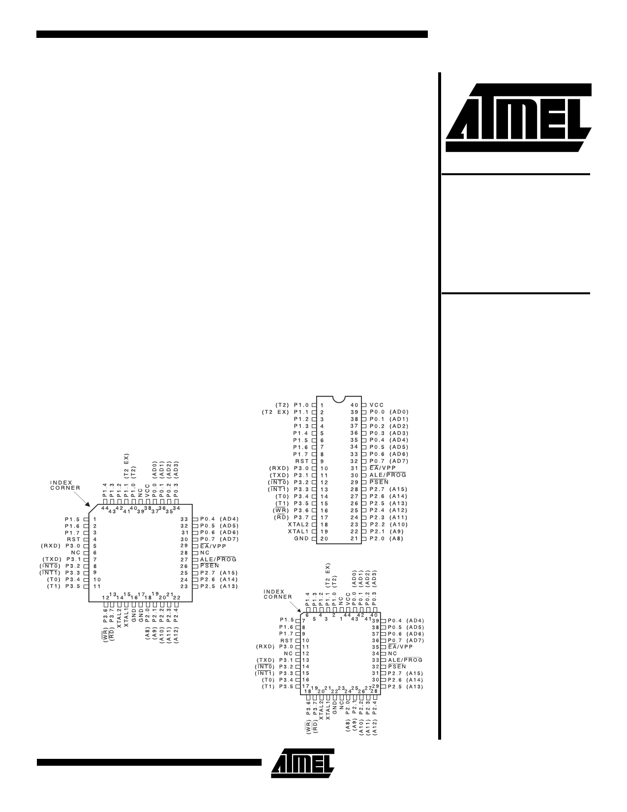
Pin Configurations
PDIP
8-Bit
Microcontroller
with 8K Bytes
Flash
AT89LV52
TQFP
PLCC
0375D-E–12/97
4-83
1 page 
AT89LV52
Special Function Registers
A map of the on-chip memory area called the Special Func-
tion Register (SFR) space is shown in Table 1.
Note that not all of the addresses are occupied, and unoc-
cupied addresses may not be implemented on the chip.
Read accesses to these addresses will in general return
random data, and write accesses will have an indetermi-
nate effect.
User software should not write 1s to these unlisted loca-
tions, since they may be used in future products to invoke
Table 2. T2CON—Timer/Counter 2 Control Register
T2CON Address = 0C8H
Bit Addressable
TF2
EXF2
RCLK
TCLK
Bit 7 6 5 4
new features. In that case, the reset or inactive values of
the new bits will always be 0.
Timer 2 Registers Control and status bits are contained in
registers T2CON (shown in Table 2) and T2MOD (shown in
Table 4) for Timer 2. The register pair (RCAP2H, RCAP2L)
are the Capture/Reload registers for Timer 2 in 16-bit cap-
ture mode or 16-bit auto-reload mode.
Interrupt Registers The individual interrupt enable bits
are in the IE register. Two priorities can be set for each of
the six interrupt sources in the IP register.
EXEN2
3
Reset Value = 0000 0000B
TR2
C/T2
CP/RL2
2 10
Symbol
TF2
EXF2
RCLK
TCLK
EXEN2
TR2
C/T2
CP/RL2
Function
Timer 2 overflow flag set by a Timer 2 overflow and must be cleared by software. TF2 will not be set when either
RCLK = 1 or TCLK = 1.
Timer 2 external flag set when either a capture or reload is caused by a negative transition on T2EX and EXEN2 = 1.
When Timer 2 interrupt is enabled, EXF2 = 1 will cause the CPU to vector to the Timer 2 interrupt routine. EXF2
must be cleared by software. EXF2 does not cause an interrupt in up/down counter mode (DCEN = 1).
Receive clock enable. When set, causes the serial port to use Timer 2 overflow pulses for its receive clock in serial
port Modes 1 and 3. RCLK = 0 causes Timer 1 overflow to be used for the receive clock.
Transmit clock enable. When set, causes the serial port to use Timer 2 overflow pulses for its transmit clock in serial
port Modes 1 and 3. TCLK = 0 causes Timer 1 overflows to be used for the transmit clock.
Timer 2 external enable. When set, allows a capture or reload to occur as a result of a negative transition on T2EX if
Timer 2 is not being used to clock the serial port. EXEN2 = 0 causes Timer 2 to ignore events at T2EX.
Start/Stop control for Timer 2. TR2 = 1 starts the timer.
Timer or counter select for Timer 2. C/T2 = 0 for timer function. C/T2 = 1 for external event counter (falling edge
triggered).
Capture/Reload select. CP/RL2 = 1 causes captures to occur on negative transitions at T2EX if EXEN2 = 1. CP/RL2
= 0 causes automatic reloads to occur when Timer 2 overflows or negative transitions occur at T2EX when EXEN2 =
1. When either RCLK or TCLK = 1, this bit is ignored and the timer is forced to auto-reload on Timer 2 overflow.
Data Memory
The AT89LV52 implements 256 bytes of on-chip RAM. The
upper 128 bytes occupy a parallel address space to the
Special Function Registers. That means the upper 128
bytes have the same addresses as the SFR space but are
physically separate from SFR space.
When an instruction accesses an internal location above
address 7FH, the address mode used in the instruction
specifies whether the CPU accesses the upper 128 bytes
of RAM or the SFR space. Instructions that use direct
addressing access SFR space.
For example, the following direct addressing instruction
accesses the SFR at location 0A0H (which is P2).
MOV 0A0H, #data
Instructions that use indirect addressing access the upper
128 bytes of RAM. For example, the following indirect
addressing instruction, where R0 contains 0A0H, accesses
the data byte at address 0A0H, rather than P2 (whose
address is 0A0H).
MOV @R0, #data
Note that stack operations are examples of indirect
addressing, so the upper 128 bytes of data RAM are avail-
able as stack space.
4-87
5 Page 
AT89LV52
Oscillator Characteristics
XTAL1 and XTAL2 are the input and output, respectively,
of an inverting amplifier that can be configured for use as
an on-chip oscillator, as shown in Figure 7. Either a quartz
crystal or ceramic resonator may be used. To drive the
device from an external clock source, XTAL2 should be left
unconnected while XTAL1 is driven, as shown in Figure 8.
There are no requirements on the duty cycle of the external
clock signal, since the input to the internal clocking circuitry
is through a divide-by-two flip-flop, but minimum and maxi-
mum voltage high and low time specifications must be
observed.
Idle Mode
In idle mode, the CPU puts itself to sleep while all the on-
chip peripherals remain active. The mode is invoked by
software. The content of the on-chip RAM and all the spe-
cial functions registers remain unchanged during this
mode. The idle mode can be terminated by any enabled
interrupt or by a hardware reset.
Note that when idle mode is terminated by a hardware
reset, the device normally resumes program execution
from where it left off, up to two machine cycles before the
internal reset algorithm takes control. On-chip hardware
inhibits access to internal RAM in this event, but access to
the port pins is not inhibited. To eliminate the possibility of
an unexpected write to a port pin when idle mode is termi-
nated by a reset, the instruction following the one that
invokes idle mode should not write to a port pin or to exter-
nal memory.
Figure 7. Oscillator Connections
C2
XTAL2
C1
XTAL1
GND
Note: C1, C2 = 30 pF ± 10 pF for Crystals
= 40 pF ± 10 pF for Ceramic Resonators
Figure 8. External Clock Drive Configuration
NC XTAL2
EXTERNAL
OSCILLATOR
SIGNAL
XTAL1
Power Down Mode
In the power down mode, the oscillator is stopped, and the
instruction that invokes power down is the last instruction
executed. The on-chip RAM and Special Function Regis-
ters retain their values until the power down mode is termi-
nated. The only exit from power down is a hardware reset.
Reset redefines the SFRs but does not change the on-chip
RAM. The reset should not be activated before VCC is
restored to its normal operating level and must be held
active long enough to allow the oscillator to restart and sta-
bilize.
GND
Status of External Pins During Idle and Power Down Modes
Mode
Idle
Idle
Power Down
Power Down
Program Memory
Internal
External
Internal
External
ALE
1
1
0
0
PSEN
1
1
0
0
PORT0
Data
Float
Data
Float
PORT1
Data
Data
Data
Data
PORT2
Data
Address
Data
Data
PORT3
Data
Data
Data
Data
4-93
11 Page | ||
| Páginas | Total 22 Páginas | |
| PDF Descargar | [ Datasheet AT89LV52-12PI.PDF ] | |
Hoja de datos destacado
| Número de pieza | Descripción | Fabricantes |
| AT89LV52-12PC | 8-Bit Microcontroller with 8K Bytes Flash | ATMEL Corporation |
| AT89LV52-12PI | 8-Bit Microcontroller with 8K Bytes Flash | ATMEL Corporation |
| Número de pieza | Descripción | Fabricantes |
| SLA6805M | High Voltage 3 phase Motor Driver IC. |
Sanken |
| SDC1742 | 12- and 14-Bit Hybrid Synchro / Resolver-to-Digital Converters. |
Analog Devices |
|
DataSheet.es es una pagina web que funciona como un repositorio de manuales o hoja de datos de muchos de los productos más populares, |
| DataSheet.es | 2020 | Privacy Policy | Contacto | Buscar |