|
|
|
PDF AT43USB353M Data sheet ( Hoja de datos )
| Número de pieza | AT43USB353M | |
| Descripción | Missed Watchdog Timer Reset | |
| Fabricantes | ATMEL Corporation | |
| Logotipo | ||
Hay una vista previa y un enlace de descarga de AT43USB353M (archivo pdf) en la parte inferior de esta página. Total 30 Páginas | ||
|
No Preview Available !
Features
• AVR® 8-bit RISC Microcontroller with 41.5 or 83 ns Instruction Cycle Time
• USB Hub with One Attached and Two External Ports
• USB Function with Three Programmable End-points
• 24 KB Program Memory, 1 KB Data SRAM
• 32 x 8 General-purpose Working Registers
• 15 Programmable I/O Port Pins
• 12-channel 10-bit ADC
• One 8-bit Timer/Counter with Separate Pre-scaler
• One 16-bit Timer/Counter with Separate Pre-scaler and Two PWMs
• External and Internal Interrupt Sources
• Programmable Watchdog Timer
• 6 MHz Oscillator with On-chip PLL
• 5V Operation with On-chip 3.3V Power Supply
• 48-lead LQFP Package
Description
The Atmel AT43USB353M is an 8-bit microcontroller based on the AVR RISC archi-
tecture. By executing powerful instructions in a single clock cycle, the AT43USB353M
achieves throughputs approaching 24 MIPS. The AVR core combines a rich instruc-
tion set with 32 general-purpose working registers. All 32 registers are directly
connected to the ALU allowing two independent registers to be accessed in one single
instruction executed in one clock cycle. The resulting architecture is more code effi-
cient while achieving throughputs up to ten times faster than conventional CISC
microcontrollers.
The AT43USB353M features an on-chip 24-Kbyte of masked ROM program memory
and 1-Kbyte of data memory. It is supported by a standwawwr.dDatsaSehetet4oUf.copmeripherals such as
timer/counter modules, watchdog timer and internal and external interrupt sources.
The major peripheral included in the AT43USB353M is a full-speed USB 2.0 Hub with
an embedded function and a 12-channel Analog-to-Digital Converter (ADC) for use in
applications such as game controllers.
The AT43USB353M is binary compatible with the AT43USB355. Program develop-
ment and debugging for the AT43USB353M uses the AT43DK355, including all its
tools and libraries.
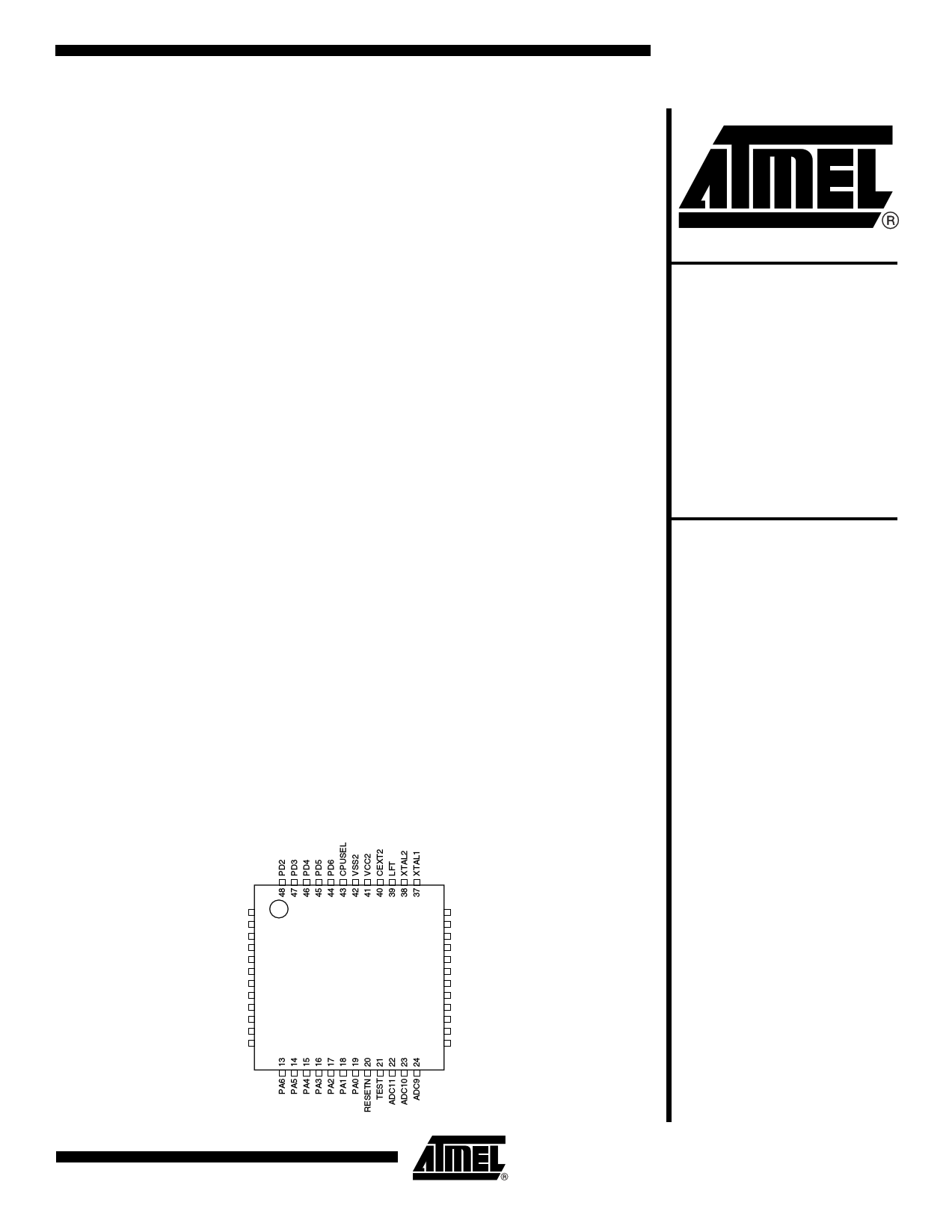
Pin Configuration
Figure 1. AT43USB353M 48-lead LQFP
Low Cost
Full-speed USB
Microcontroller
with Embedded
Hub, ADC and
PWM
AT43USB353M
PD1
PD0
DP3
DM3
DP2
DM2
DP0
DM0
CEXT1
VCC1
VSS1
PA7
1
2
3
4
5
6
7
8
9
10
11
12
36 VSSA
35 CEXTA
34 VCCA
33 ADC0
32 ADC1
31 ADC2
30 ADC3
29 ADC4
28 ADC5
27 ADC6
26 ADC7
25 ADC8
Rev. 3307B–USB–4/04
1
1 page 
3307B–USB–4/04
AT43USB353M
The embedded USB hardware of the AT43USB353M is a compound device, consisting of a 3
port hub with a permanently attached function on one port. The hub and attached function are
two independent USB devices, each having its own device addresses and control end-points.
The hub has its dedicated interrupt end-point, while the USB function has 3 additional pro-
grammable end-points with separate FIFOs. Two of the FIFOs are 64 bytes deep and the third
is 8 bytes deep.
Depending on the state of the CPUSEL input pin, device pin 43, the MCU runs at 12 MHz or
24 MHz. The clock that operates the MCU is generated by the USB hardware. While at
12 MHz the nominal and average period of the clock is 83.3 ns. It may have single cycles that
deviate by ±20.8 ns during a phase adjustment by the SIE's clock/data separator of the USB
hardware. The 24 MHz clock runs with a clock period of 41.67 ns that may increase to 62.5 ns
for one cycle when the SIE's clock/data separator makes an adjustment. The clock frequen-
cies of the various modules of the AT43USB353M is summarized in Table 1.
Table 1. Module Clock Frequencies
CPUSEL Pin MCU Clock
Timer/Counter Clock
ADC Clock
WDT Clock
0 24 MHz
12 MHz
1 MHz
1 MHz
1 12 MHz
12 MHz
1 MHz
1 MHz
Note: Refer to page 15 for details of the on chip oscillator and PLL.
The microcontroller shares most of the control and status registers of the megaAVR Microcon-
troller Family. The registers for managing the USB operations are mapped into its SRAM
space. The I/O section on page 13 summarizes the available I/O registers. The “AVR Register
Set” on page 32 covers the AVR registers. Please refer to the Atmel AVR manual for more
information.
The fast-access register file concept contains 32 x 8-bit general-purpose working registers
with a single clock cycle access time. This means that during one single clock cycle, one Arith-
metic Logic Unit (ALU) operation is executed. Two operands are output from the register file,
the operation is executed, and the result is stored back in the register file – in one clock cycle.
Six of the 32 registers can be used as three 16-bit indirect address register pointers for Data
Space addressing - enabling efficient address calculations. One of the three address pointers
is also used as the address pointer for look-up tables in program memory. These added func-
tion registers are the 16-bit X-, Y- and Z-registers.
The ALU supports arithmetic and logic operations between registers or between a constant
and a register. Single register operations are also executed in the ALU. Figure 2 on page 4
shows the AT43USB353M AVR Enhanced RISC microcontroller architecture.
In addition to the register operation, the conventional memory addressing modes can be used
on the register file as well. This is enabled by the fact that the register file is assigned the 32
lowest Data Space addresses ($00 - $1 F), allowing them to be accessed as though they were
ordinary memory locations.
The I/O memory space contains 64 addresses for CPU peripheral functions as Control Regis-
ters, Timer/Counters, and other I/O functions. The I/O Memory can be accessed directly, or as
the Data Space locations following those of the register file, $20 - $5F.
The AVR uses a Harvard architecture concept – with separate memories and buses for pro-
gram and data. The program memory is executed with a single-level pipelining. While one
instruction is being executed, the next instruction is pre-fetched from the program memory.
This concept enables instructions to be executed in every clock cycle. The program memory is
a downloadable SRAM or a mask programmed ROM.
5
5 Page 
AT43USB353M
Table 5. USB Hub and Function Registers (Continued)
Address
Name
Function
$1FBA
HPSTAT3
Hub Port 3 Status Register
$1FB9
HPSTAT2
Hub Port 2 Status Register
$1FB8
HPSTAT1
Hub Port 1 Status Register
$1FB2
HPSCR3
Hub Port 3 Status Change Register
$1FB1
HPSCR2
Hub Port 2 Status Change Register
$1FB0
HPSCR1
Hub Port 1 Status Change Register
$1FAA
PSTATE3
Hub Port 3 Bus State Register
$1FA9
PSTATE2
Hub Port 2 Bus State Register
$1FA7
HCAR0
Hub End-point 0 Control and Acknowledge Register
$1FA5
FCAR0
Function End-point 0 Control and Acknowledge Register
$1FA4
FCAR1
Function End-point 1 Control and Acknowledge Register
$1FA3
FCAR2
Function End-point 2 Control and Acknowledge Register
$1FA2
FCAR3
Function End-point 3 Control and Acknowledge Register
3307B–USB–4/04
11
11 Page | ||
| Páginas | Total 30 Páginas | |
| PDF Descargar | [ Datasheet AT43USB353M.PDF ] | |
Hoja de datos destacado
| Número de pieza | Descripción | Fabricantes |
| AT43USB353M | Missed Watchdog Timer Reset | ATMEL Corporation |
| Número de pieza | Descripción | Fabricantes |
| SLA6805M | High Voltage 3 phase Motor Driver IC. |
Sanken |
| SDC1742 | 12- and 14-Bit Hybrid Synchro / Resolver-to-Digital Converters. |
Analog Devices |
|
DataSheet.es es una pagina web que funciona como un repositorio de manuales o hoja de datos de muchos de los productos más populares, |
| DataSheet.es | 2020 | Privacy Policy | Contacto | Buscar |